Rigid PCB Capabilities
Items | Standard | Advanced | Remarks |
Number of Layers | 1-24 layer | 1-30 layer | For orders above 24layers, please contact our sales rep. |
Material | standard FR-4,CEM-1,CEM-3,FR1 | Rogers/Teflon | For example: |
Maximum PCB Size(Dimension) | 500*600mm | 1000*600mm | For any sizes beyond this dimension, please contact the sales rep. |
Board Size Tolerance | ±0.13mm | +/-0.1mm for CNC routing +/-0.05mm for laser routing | ±0.1mm for CNC routing, and ±0.15mm for V-scoring. |
Board Thickness | 0.1-3.2mm | 0.1-7mm | 0.1-7mm. Please view the below "Standard PCB" or contact us if your board exceeds these. |
Board Thickness | ±10% | +/-8% | Normally “+ Tolerance” will occur due to PCB processing steps such as electroless copper, solder mask, and other types of finish on the surface. |
Board Thickness | ±0.1mm | +/-0.05mm | |
Min Trace | 3.5mil | 3mil | Min manufacturable trace is 3mil(0.075mm), strongly suggest designing trace above 3.5mil(0.09mm) to save cost. |
Min Spacing | 3.5mil | 3mil | Min manufacturable spacing is 3mil(0.075mm), strongly suggest designing spacing above 3.5mil(0.09mm) to save cost. |
Outer Layer Copper Thickness | 6oz | 10oz | Also known as copper weight. 35μm=1oz, 70μm=2oz, 105μm=3oz. Please contact us if you need copper weight greater than 6oz. |
Inner Layer Copper Thickness | 4oz | 6oz | Inner copper weight as per customer’s request for 4 and 6 layers(Multi-layer laminated structure). Please contact us if you need copper weight greater than 6oz. |
Drill Sizes (CNC) | 0.2-6.0mm | 0.15-6.5mm | Min drill size is 0.15mm, max drill is 6.5mm. Any holes greater than 6.0mm or smaller than 0.3mm will be subject to extra charges. |
Min Width of Annular Ring | 0.15mm | 0.1mm | For pads with vias in the middle, Min width for Annular Ring is 0.1mm(4mil). |
Finished Hole Diameter (CNC) | 0.2-6.0mm | 0.15-6.5mm | The finished hole diameter will be smaller than size of the drill bits because of the copper plating in the hole barrels |
Finished Hole Size Tolerance(CNC) | ±0.076mm | +/-0.05mm | min±0.05mm |
Solder Mask(type) | LPI | UV | Liquid Photo-Imageable is mostly adopted. Thermosetting Ink is used in inexpensive paper-based boards. |
Minimum Character Width(Legend) | 0.2mm | 0.12mm | Characters of less than 0.12mm wide will be too narrow to be identifiable. |
Minimum Character Height (Legend) | 0.8mm | 0.71mm | Characters of less than 0.71mm high will be too small to be recognizable. |
Character Width to Height Ratio (Legend) | 4:1 | 5:1 | In PCB silkscreen legends processing, 1:5 is the most suitable ratio |
Minimum Diameter of Plated Half Holes | 0.5mm | 0.45mm | Design Half-Holes greater than 0.5mm to ensure a better connection between boards. |
Surface Finishing | HASL(1-40um) |
| The most popular three types of PCB surface finish. |
Solder Mask (color) | White,Black,yellow,green, |
| The most popular four colors of PCB solder mask. |
Silkscreen (color) | White,Black,yellowgreen, blue,grey,red,purple |
| The most popular two colors of PCB solder mask. |
Panelization (type) | V-scoring,Tab-routing, Tab-routing with Perforation (Stamp Holes) |
| Leave min clearance of 1.0mm between boards for break-routing. For V-score penalization, set the space between boards to zero. |
Others | Fly Probe Testing A.O.I. E-testing |
|
|
Qualification | UL Certified ISO9001/ISO13485/TS16949 |
|
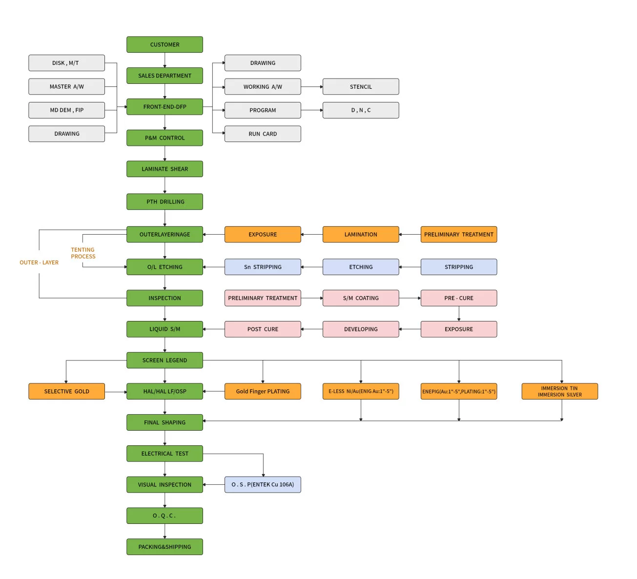
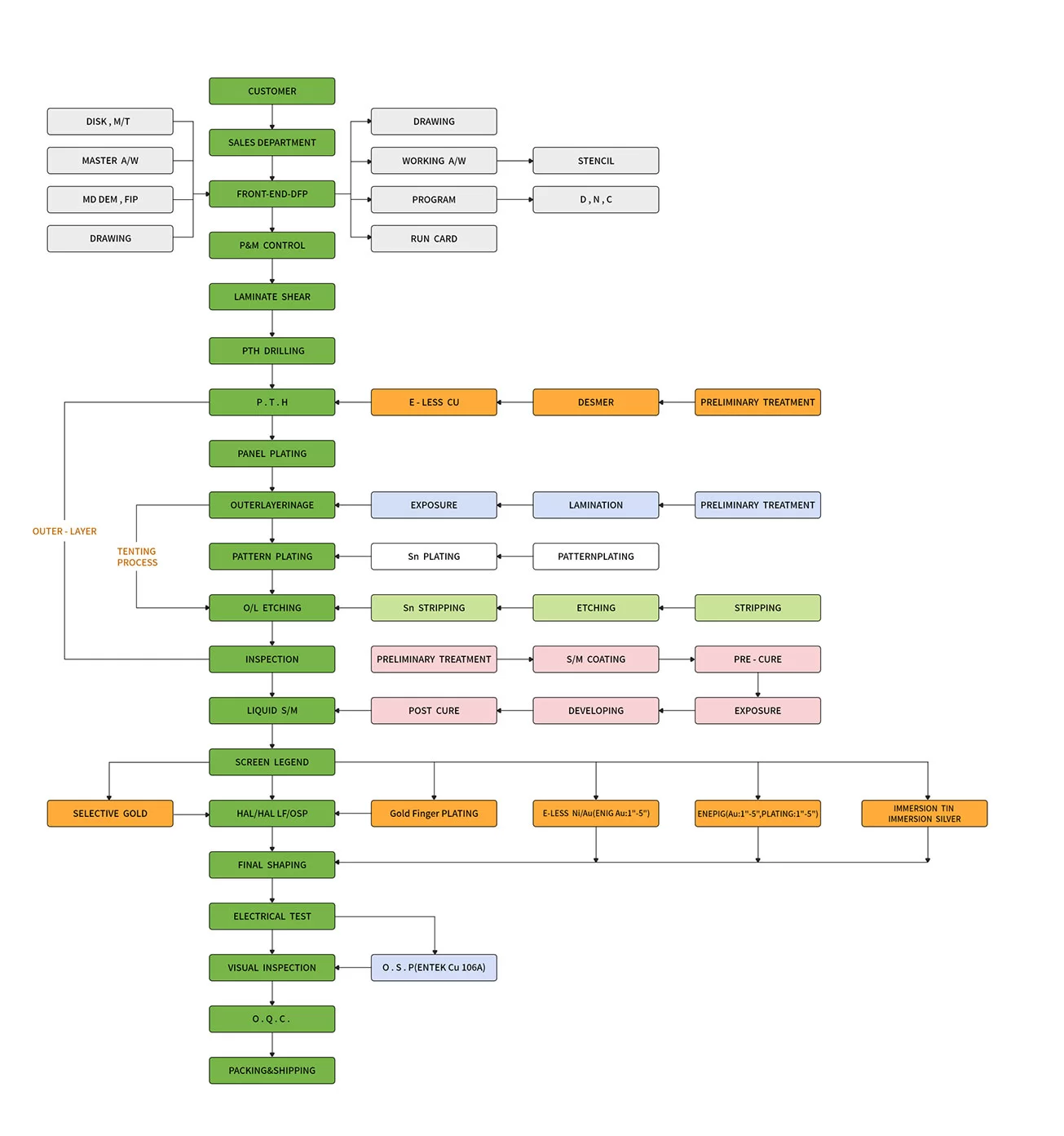
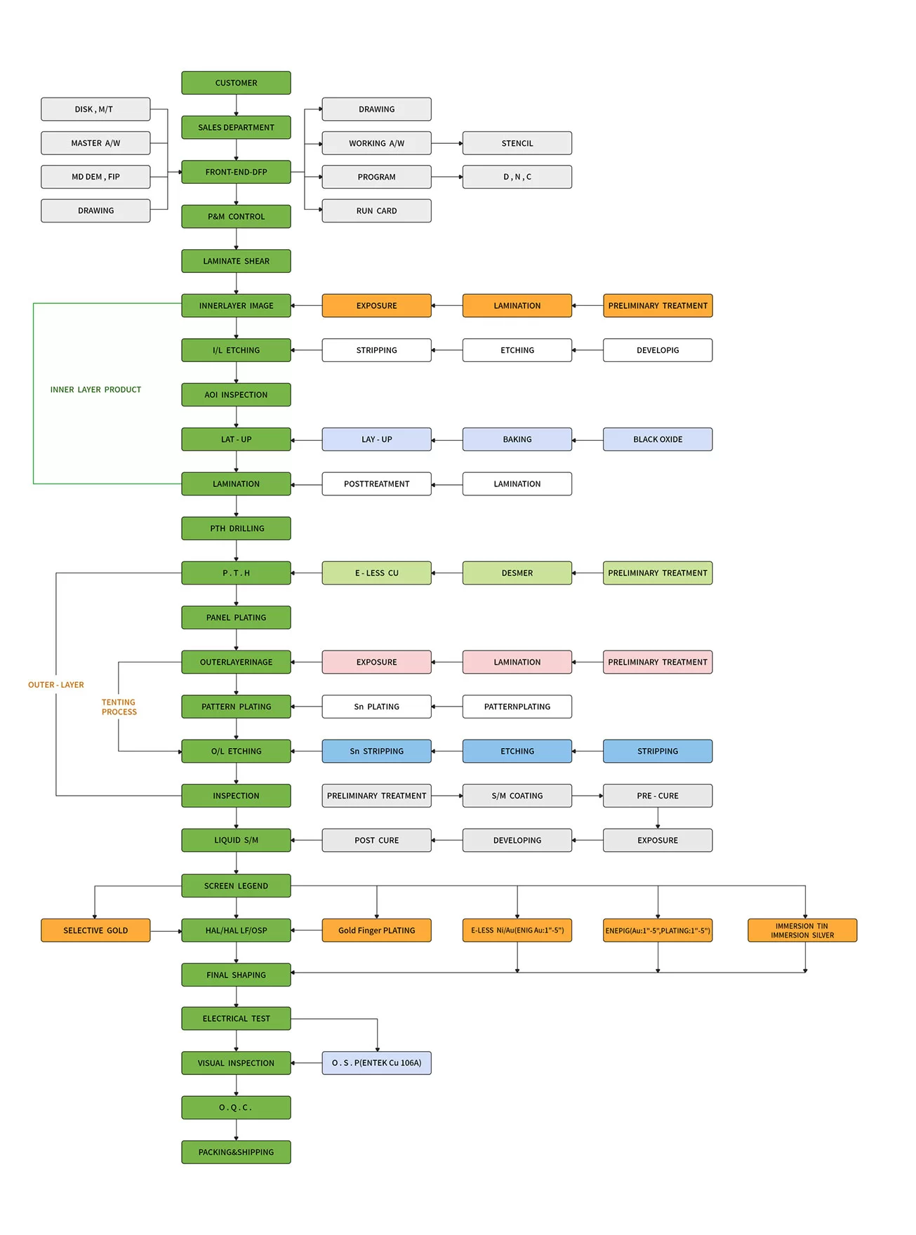
Rigid PCB Manufacturing Process is a process of producing printed circuit boards (PCB) with a rigid surface material. It involves several processes to ensure the PCBs are produced with the highest quality. The first step is to create the PCB layout. This is done using a CAD program or by hand. The layout is then used to create a mask, which is used to etch the copper traces onto the substrate. The substrate is then laminated with the desired dielectric material and the copper traces are etched onto it. The holes are drilled and the components are soldered onto the board. The boards are then tested and inspected to make sure they meet the design specifications. After this, the boards are inspected and tested again before being sent out for final assembly. The final step is to encapsulate the boards in a protective material like epoxy or solder mask to protect the boards from physical and electrical damage.
Advantages of Our Rigid PCB Capabilities
Our rigid PCB capabilities offer several advantages for customers. Firstly, we are able to provide a high level of accuracy and reliability in the production process. Our boards are designed with high-precision components and tightly controlled manufacturing processes, which ensures that all PCBs meet the highest standards of quality. Additionally, our rigid PCBs are highly durable and are able to withstand harsh environmental conditions. We offer a wide range of materials, such as FR-4, High-Tg, Polyimide and Rogers, which give our customers the flexibility to choose the most suitable material for their project. Furthermore, our lead times are shorter than most competitors, allowing customers to get their boards quickly. Finally, our prices are competitive and we offer discounts for large volume orders. All these advantages make our rigid PCB capabilities the best choice for customers.
Features of Our Rigid PCB Capabilities
Rigid PCB Capabilities from Golden Triangle are the best choice for electronics manufacturers who require reliable and high-quality printed circuit boards. With an extensive range of capabilities, Golden Triangle is the ideal choice for any project, from high-performance consumer electronics applications to specialized industrial applications.Golden Triangle offers a wide range of rigid PCB capabilities, from quick-turn prototype builds to high-volume production runs. The company's advanced capabilities include multilayer PCBs, impedance control, HDI (high-density interconnect) designs, and rigorous quality control. Golden Triangle's multilayer PCBs can support up to 32 layers, allowing for complex designs with tight tolerances. The company's HDI designs are capable of incorporating up to six layers of copper, allowing for greater circuit density.
Single-layer Process

Double-layer Process

Multilayer Process


