Copper PCB Capabilities
Items | Standard | Advanced | Remarks |
Number of Layers | 1-2L | 1-6L | For orders above 6layers, please contact our sales rep. |
Material | AL base | AL base |
|
Maximum PCB Size | 500*600mm | 1300*600mm | For any sizes beyond this dimension, please view the below "Standard PCB" or contact sales re |
Board Size Tolerance | ±0.15mm | +/-0.13mm | ±0.15mm for CNC routing, and ±0.2mm for V-scoring. |
Board Thickness | 0.6-2.0mm | 0.4-3.0mm | 0.6-3mm, Please contact us if your board exceeds these. |
Board Thickness | ±10% | +/-8% | Normally “+ Tolerance” will occur due to PCB processing steps such as electroless copper, solder mask and other types of finish on the surface. |
Board Thickness | ±0.1mm | +/-0.08mm | |
Min Trace | 0.2mm | 0.15mm | Min manufacturable trace is 5.9mil(0.15mm), strongly suggest designing trace above 8mil(0.2mm) to save cost. |
Min Spacing | 0.2mm | 0.15mm | Min manufacturable spacing is 5.9mil(0.15mm), strongly suggest designing spacing above 8mil(0.2mm) to save cost. |
Outer Layer Copper Thickness | 1/2-3oz | 1/2-6oz | Also known as copper weight. 35μm=1oz.70um=2oz,105um=3oz。 Please contact us if you need copper weight greater than 6oz. |
Inner Layer Copper Thickness | 1/2-3oz | 1/2-6oz | Please contact us if you need copper weight greater than 6oz. |
Drill Sizes (CNC) | 1.0-6.0mm | 0.8-6.5mm | Min drill size is 0.8mm, max drill is 6.0mm. Any holes greater than 6.0mm or smaller than 0.3mm will be subject to extra charges. |
Min Width of Annular Ring | 0.3mm | 0.2mm | For pads with vias in the middle, Min width for Annular Ring is 0.1mm(4mil). |
Finished Hole Diameter (CNC) | 1.0mm | 0.8mm | The finished hole diameter will be smaller than size of drill bits because of copper plating in the hole barrels |
Finished Hole Size Tolerance(CNC) | ±0.1 mm | +/-0.075mm | min±0.075mm |
Solder Mask(type) | LPI | UV | Liquid Photo-Imageable is mostly adopted. Thermosetting Ink is used in inexpensive paper-based boards. |
Minimum Character Width(Legend) | 0.2mm | 0.15mm | Characters of less than 0.15mm wide will be too narrow to be identifiable. |
Minimum Character Height (Legend) | 0.8 | 0.8 | Characters of less than 0.8mm high will be too small to be recognizable. |
Character Width to Height Ratio (Legend) | 4:1 | 5.3:1 | In PCB silkscreen legends processing, 1:5.3 is the most suitable ratio |
Minimum Diameter of Plated Half Holes | 0.5 |
| Design Half-Holes greater than 0.5mm to ensure a better connection between boards. |
Surface Finishing | HASL(1-40um) |
| The most popular three types of PCB surface finish. |
Solder Mask(color) | White, Black, yellow,green,blue, |
|
|
Silkscreen(color) | White, Black, yellow,green,blue |
|
|
Panelization | V-scoring, Tab-routing, Tab-routing with Perforation (Stamp Holes) |
| Leave min clearance of 1.0mm between boards for break-routing. For V-score penalization, set the space between boards to zero. |
Others | Fly Probe Testing and A.O.I. testing(free), ISO 9001:2008 ,UL Certificate、ipc 6012/600 |
|
Overview
Copper PCBs are widely used in the electronics industry due to their superior electrical performance and durability.
The process for Manufacturing Copper PCBs
The manufacturing process for copper PCBs involves several steps. First, the circuit patterns are printed onto a copper-clad laminate using a photolithography process. Then, the printed circuit board is etched with an acid to remove the unwanted copper and leave the desired circuit pattern. After etching, the board is drilled with holes to accommodate the components. Finally, the board is plated with a thin layer of copper to protect against oxidation and provide reliable electrical contact. The board is then ready for component assembly. By following these steps, copper PCBs can be manufactured quickly and reliably with a high level of precision.
Advantages of Our Copper PCB Capabilities
Our copper PCB capabilities provide a number of advantages. Firstly, copper PCBs are highly durable, making them ideal for long-term applications. They are also resistant to corrosion, making them suitable for use in challenging environmental conditions. Copper PCBs also offers excellent electrical conductivity, allowing for high-performance circuit designs. Additionally, copper PCBs are compatible with a wide range of components, making them a versatile choice for many applications. Finally, copper PCBs can be manufactured in a variety of sizes and shapes, making them suitable for even the most complex designs. All of these advantages make copper PCB a great choice for many applications.
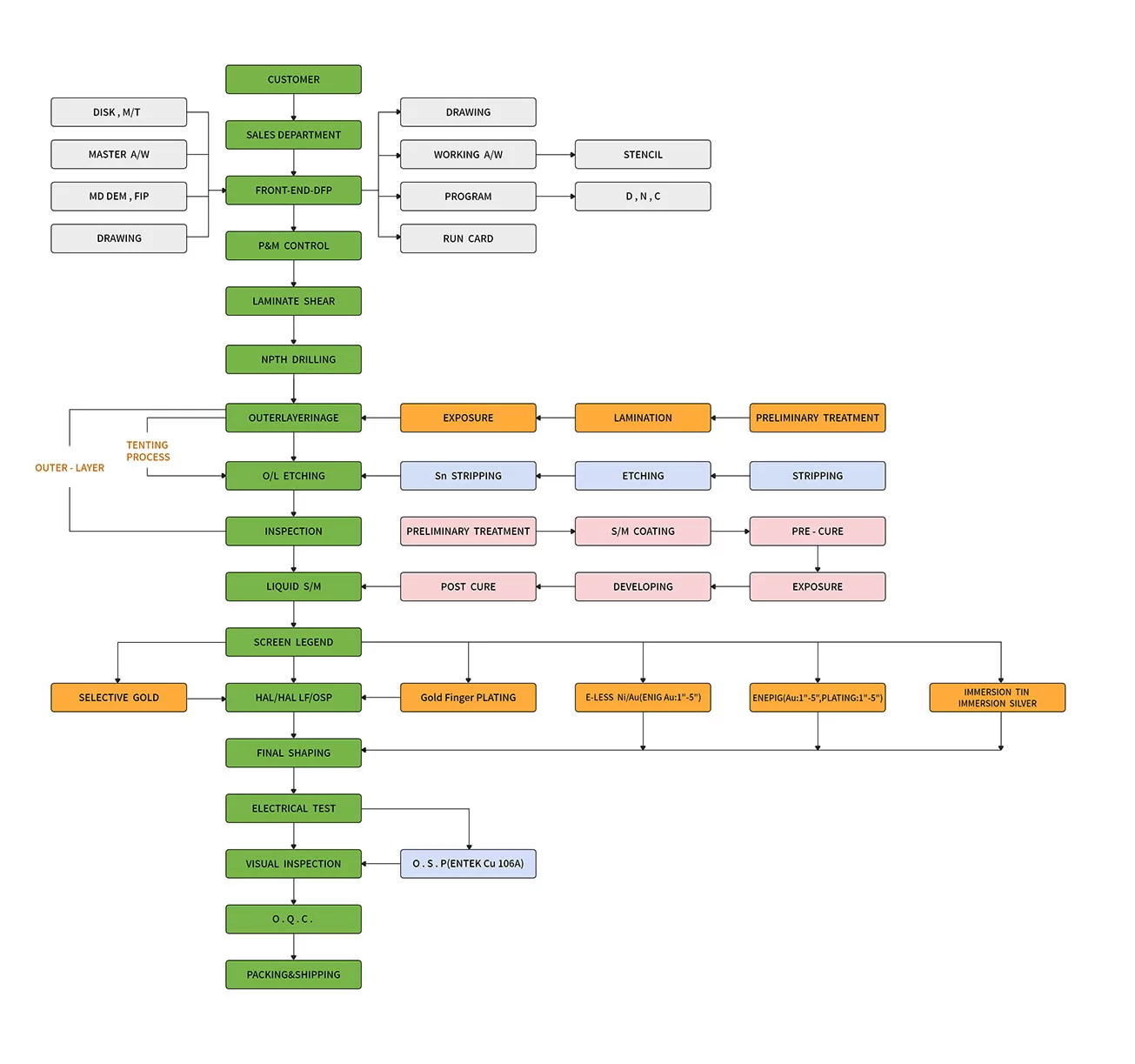
Single Layer Process

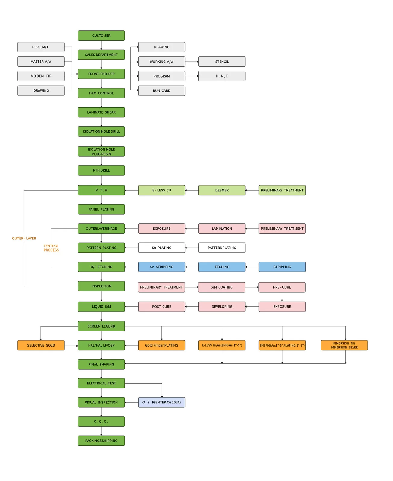
Double-layer Double-Side Process

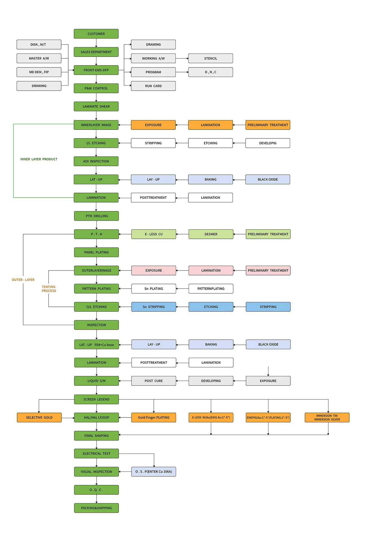
Multilayer Process


