Aluminum PCB Capabilities
Items | Standard | Advanced | Remarks |
Number of Layers | 1-2L | 1-6L | For orders above 6layers, please contact our sales rep. |
Material | AL base | AL base |
|
Maximum PCB Size | 500*600mm | 1300*600mm | For any sizes beyond this dimension, please view the below "Standard PCB" or contact sales re |
Board Size Tolerance | ±0.15mm | +/-0.13mm | ±0.15mm for CNC routing, and ±0.2mm for V-scoring. |
Board Thickness | 0.6-2.0mm | 0.4-3.0mm | 0.6-3mm, Please contact us if your board exceeds these. |
Board Thickness | ±10% | +/-8% | Normally “+ Tolerance” will occur due to PCB processing steps such as electroless copper, solder mask and other types of finish on the surface. |
Board Thickness | ±0.1mm | +/-0.08mm | |
Min Trace | 0.2mm | 0.15mm | Min manufacturable trace is 5.9mil(0.15mm), strongly suggest designing a trace above 8mil(0.2mm) to save cost. |
Min Spacing | 0.2mm | 0.15mm | Min manufacturable spacing is 5.9mil(0.15mm), strongly suggest designing spacing above 8mil(0.2mm) to save cost. |
Outer Layer Copper Thickness | 1/2-3oz | 1/2-6oz | Also known as copper weight. 35μm=1oz.70um=2oz,105um=3oz。 Please contact us if you need copper weight greater than 6oz. |
Inner Layer Copper Thickness | 1/2-3oz | 1/2-6oz | Please contact us if you need copper weight greater than 6oz. |
Drill Sizes (CNC) | 1.0-6.0mm | 0.8-6.5mm | Min drill size is 0.8mm, max drill is 6.0mm. Any holes greater than 6.0mm or smaller than 0.3mm will be subject to extra charges. |
Min Width of Annular Ring | 0.3mm | 0.2mm | For pads with vias in the middle, Min width for Annular Ring is 0.1mm(4mil). |
Finished Hole Diameter (CNC) | 1.0mm | 0.8mm | The finished hole diameter will be smaller than the size of the drill bits because of the copper plating in the hole barrels |
Finished Hole Size Tolerance(CNC) | ±0.1 mm | +/-0.075mm | min±0.075mm |
Solder Mask(type) | LPI | UV | Liquid Photo-Imageable is mostly adopted. Thermosetting Ink is used in inexpensive paper-based boards. |
Minimum Character Width(Legend) | 0.2mm | 0.15mm | Characters of less than 0.15mm wide will be too narrow to be identifiable. |
Minimum Character Height (Legend) | 0.8 | 0.8 | Characters of less than 0.8mm high will be too small to be recognizable. |
Character Width to Height Ratio (Legend) | 4:1 | 5.3:1 | In PCB silkscreen legends processing, 1:5.3 is the most suitable ratio |
Minimum Diameter of Plated Half Holes | 0.5 |
| Design Half-Holes greater than 0.5mm to ensure a better connection between boards. |
Surface Finishing | HASL(1-40um) |
| The most popular three types of PCB surface finish. |
Solder Mask(color) | White, Black, yellow,green,blue,grey,red,purple,and matt color |
|
|
Silkscreen(color) | White, Black, yellow,green,blue,grey,red,purple |
|
|
Panelization | V-scoring, Tab-routing, Tab-routing with Perforation (Stamp Holes) |
| Leave min clearance of 1.0mm between boards for break-routing. For V-score penalization, set the space between boards to be zero. |
Others | Fly Probe Testing and A.O.I. testing(free), ISO 9001:2008 ,UL Certificate、ipc 6012/600 |
|
Overview
Aluminum PCBs are created by bonding a layer of aluminum onto a substrate material. This layer of aluminum provides increased thermal performance, electrical conductivity, and mechanical strength. It also provides a higher level of corrosion resistance than traditional copper-based PCBs. The aluminum layer also helps to reduce the weight of the PCB, which is especially important in applications like aerospace and automotive.
The Process of Manufacturing Aluminum PCB
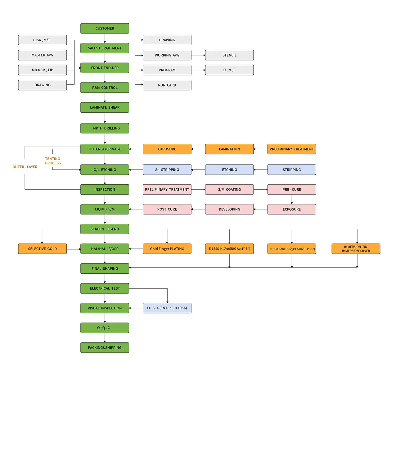
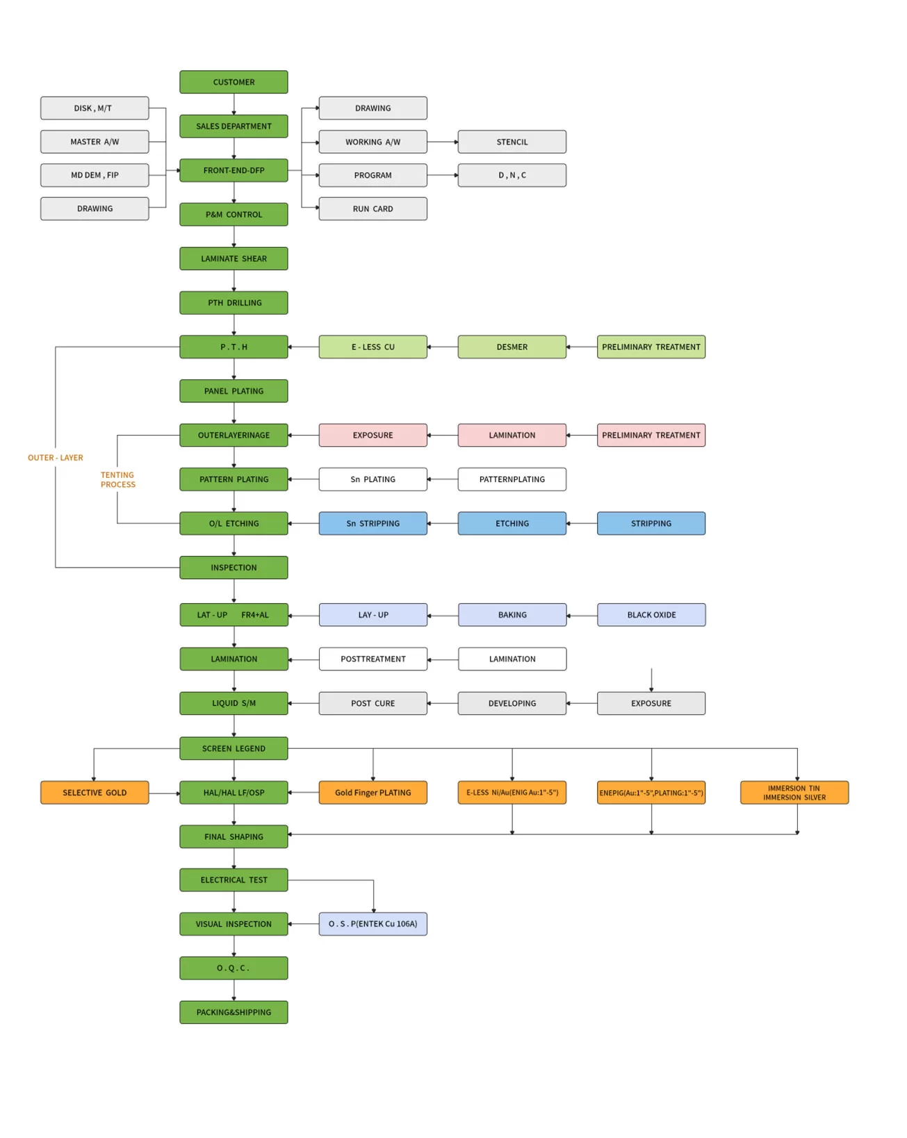
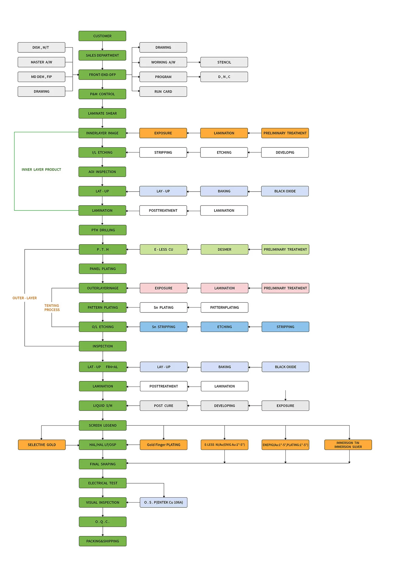
The Aluminum PCB manufacturing process consists of several steps such as PCB design, drilling, milling, plating, assembling, and testing. First, the PCB is designed on a computer, taking into account factors such as the desired board size and the number of components needed. Next, the board is drilled and milled with precision to create the circuit pathways. After that, a protective layer of copper is plated onto the board to ensure its electrical conductivity. Then, components are soldered onto the board. Finally, the board is tested for functionality and quality. This process is used to create durable and reliable aluminum PCBs for various applications.
Advantages of Our Aluminum PCB Capabilities
Our aluminum PCB capabilities offer many advantages. Firstly, aluminum PCBs have higher thermal conductivity than FR4 PCBs, allowing for excellent heat dissipation, which is especially beneficial for applications with high power consumption. Furthermore, these PCBs are lightweight and durable, making them ideal for applications that require a low-weight and reliable circuit. Additionally, aluminum PCBs provide superior electrical insulation, reducing the risk of short circuits and providing a long service life. Finally, aluminum PCBs are more cost-effective than other PCBs, making them a great choice for tight budgets. With these advantages, our aluminum PCB capabilities provide the perfect solution for a wide range of applications.
Single Layer Process

Double-layer Single-Side Process

Multilayer Process


