Flex PCB Capabilities
Items | Standard | Advanced | Remarks |
Number of Layers | 0-4L | 0-6L | For orders above 6 layers, please contact our sales rep. |
Material | Polyimide | PET | For example:Dupont, shengyi, Taiflex, Iteq, etc. |
Maximum PCB Size | 480*480mm | 1200*480mm | Raw material width is only two types 250/500mm, penalization should be based on the above two sizes, for any sizes beyond this dimension, please contact sales. |
Board Size Tolerance | ±0.10mm for punching | +/-0.05mm fo r laser cutting | ±0.05mm for laser routing, and ±0.1mm for Die punching. |
Board Thickness | 0.05-0.3mm | 0.05-0.75mm | 0.05-0.75mm. Please view the below "Standard PCB" or contact us if your board exceeds these. |
Board Thickness | ±0.05mm | ±0.03mm | min±0.03mm Normally “+ Tolerance” will occur due to PCB processing steps such as electroless copper, solder mask and other types of finish onthe surface. |
Min Trace | 3mil | 1mil | Min manufacturable trace is 1mil(0.025mm), strongly suggest designing trace above 3mil(0.0.75mm) to save cost. |
Min Spacing | 3mil | 1mil | Min manufacturable spacing is 1mil(0.025mm), strongly suggest designing spacing above 3mil(0.0.75mm) to save cost. |
Outer Layer Copper Thickness | 1/3-2oz | 1/3-3oz | Also known as copper weight. 35μm=1oz. Please view the below "Standard PCB" or contact us if you need copper weight greater than 3oz. |
Inner Layer Copper Thickness | 1/3-2oz | 1/3-3oz | Inner copper weight as per customer's request for 4 and 6 layers(Multi-layer laminated structure). Please contact us if you need copper weight greater than 3oz. |
Drill Sizes (CNC) | 0.2-6.0mm | 0.1-6.5mm | Min drill size is 0.1mm, max drill is 6.5mm. Any holes greater than 6.5mm or smaller than 0.3mm will be subject to extra charges. |
Min Width of Annular Ring | 0.15mm | 0.1mm | For pads with vias in the middle, Min width for Annular Ring is 0.1mm(4mil). |
Finished Hole Diameter (CNC) | 0.05-6.0mm | 0.05-6.5mm | The finished hole diameter will be smaller than the size of the drill bits because of the copper plating in the hole barrels |
Finished Hole Size Tolerance(CNC) | +/-0.076mm | +/-0.05mm | min±0.05mm For example, if the drill size is 0.6mm, the finished hole diameter ranges from 0.525mm to 0.675mm will be considered acceptable. |
Solder Mask(type) | coverlay | LPI solder mask ink | Liquid Photo-Imageable is mostly adopted. |
Minimum Character Width(Legend) | 0.2mm | 0.127mm | Characters of less than 0.127mm wide will be too narrow to be identifiable. |
Minimum Character Height (Legend) | 0.8mm | 0.71mm | Characters of less than 0.71mm high will be too small to be recognizable. |
Character Width to Height Ratio (Legend) | 4:01 | 5.6:1 | In PCB silkscreen legends processing, 1:5.6 is the most suitable ratio |
Minimum Diameter of Plated Half Holes | 0.5mm |
| Design Half-Holes greater than 0.5mm to ensure a better connection between boards. |
Surface Finishing | Immersion Au (1-5u"), |
| The most popular two types of PCB surface finish. Immersion Au (1-5u"), OSP(0.12um minimum) |
coverlay(color) | White, Black, yellow |
|
|
Solder Mask(color) | White, Black, yellow, |
|
|
Silkscreen(color) | White, Black, yellow, green,blue,grey,red, purple |
|
|
Panelization(type) | Tab-routing, Tab-routing with Perforation (Stamp Holes) |
| Leave min clearance of 1.0mm between boards for break-routing. For V-score penalization, set the space between boards to zero. |
Others | Fly Probe Testing |
|
|
Qualification | UL Certified ISO9001 ISO13485/TS16949 Reach RoHS IPC PPAP IMDS |
|
Overview
Flex PCB Manufacturing Process is a form of Printed Circuit Board (PCB) that is made of flexible, instead of rigid, material. This type of PCB is used for a variety of applications, such as medical and automotive, as it is capable of being bent or folded and is also lightweight.
The process for Manufacturing Flex PCBs
The process for manufacturing flex PCBs involves making a design with a CAD program, followed by fabrication of the PCB, which is done by laminating thin layers of copper foil onto the flex material. The copper layers are then patterned with a photolithography process, where an etching mask is used to create the desired circuitry pattern. Then the copper layers are etched with a chemical or mechanical process to remove the unwanted copper, leaving the desired circuitry pattern. Finally, a solder mask is applied to the board and the components are soldered on to complete the board.
Advantages of Our Flex PCB Capabilities
1. Advanced manufacturing techniques: Our flex PCB capabilities utilize the latest advanced manufacturing techniques to achieve better accuracy, reliability, and quality.
- 2. Advanced testing methods: We employ rigorous quality assurance processes and advanced testing methods to ensure that our flex PCBs are of the highest quality.
- 3. Design flexibility: Our flex PCBs are highly customizable and provide design flexibility to meet customer requirements.
- 4. Cost-effectiveness: Our flex PCBs are cost-effective, providing savings in materials, labor, and overall production costs.
- 5. Small size: Our flex PCBs are small in size, allowing them to fit into tight spaces and enabling them to be used in a variety of applications.
- 6. Durability: Our flex PCBs are highly durable, providing resistance to vibrations, shocks, and electrical changes.
- 7. High-speed performance: Our flex PCBs provide high-speed performance and can handle high data transfer rates.
- 8. Reduced component count: Our flex PCBs require fewer components than standard PCBs, reducing overall assembly costs.
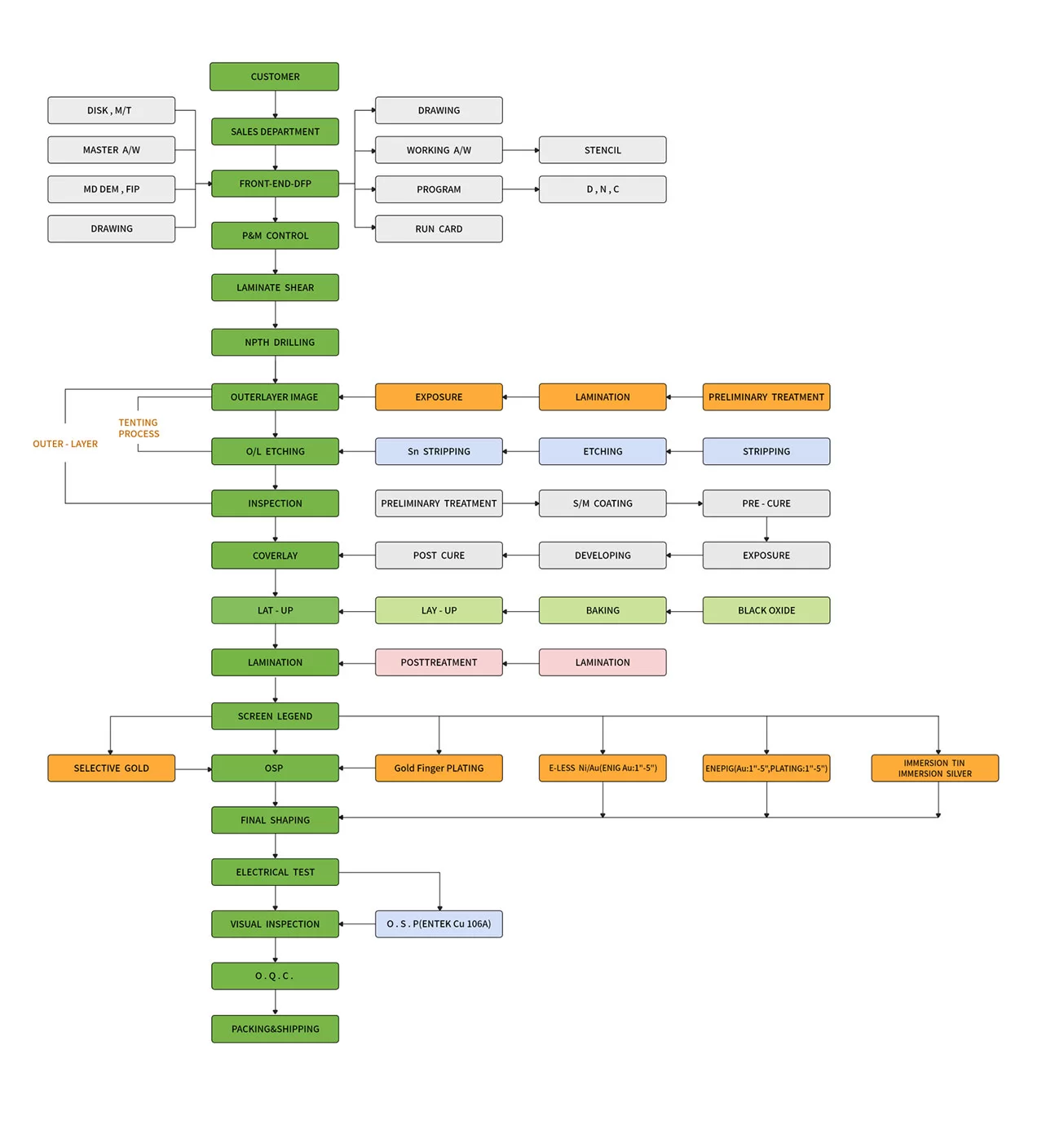
Single-layer Process

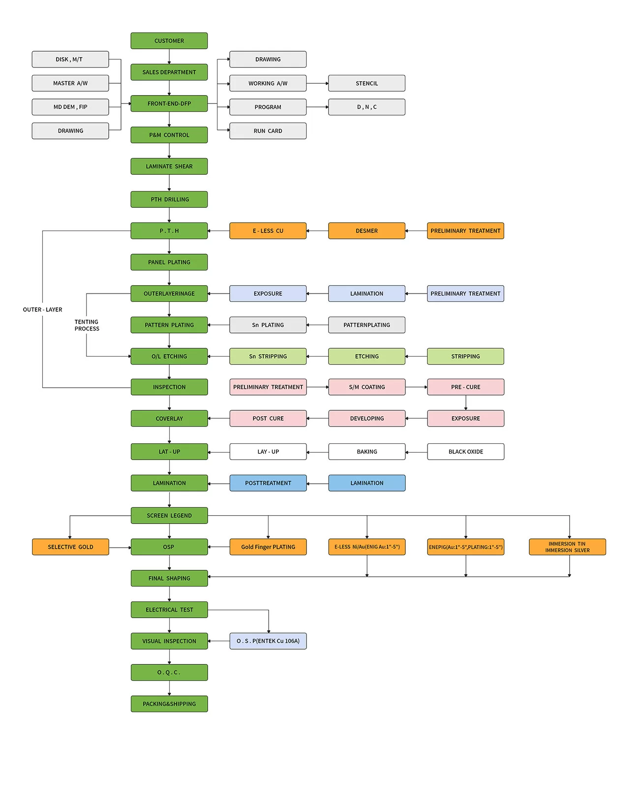
Double-layer Process

Multilayer Process


