Rigid-Flex PCB Capabilities
Items | Standard | Remarks |
Number of Layers | 2-10 | For orders above 10 layers, please view the below "Standard PCB" or contact our sales rep. |
Material | FR4+Polyimide | For Halogen-free, High Tg, etc., please view the below "Standard PCB" or contact the sales rep. |
Maximum PCB Size | 280*450mm | For any sizes beyond this dimension, please view the below "Standard PCB" or contact sales re |
Board Size Tolerance | ±0.10mm | ±0.1mm for CNC routing, and ±0.5mm for V-scoring. |
Board Thickness | 0.6-2.5mm | 0.6-2.5mm. Please view the below "Standard PCB" or contact us if your board exceeds these. |
Board Thickness | ±10% | Normally “+ Tolerance” will occur due to PCB processing steps such as electroless copper, solder mask and other types of finish on the surface. |
Board Thickness | ±0.10mm | |
Min Trace | 3mil | Min manufacturable trace is 3mil(0.075mm), strongly suggest designing trace above 4mil(0.1mm) to save cost. |
Min Spacing | 3mil | Min manufacturable spacing is 3mil(0.075mm), strongly suggest designing spacing above 4mil(0.1mm) to save cost. |
Outer Layer Copper Thickness | 1/2-3oz | Also known as copper weight. 35μm=1oz. Please view the below "Standard PCB" or contact us if you need copper weight greater than 3oz. |
Inner Layer Copper Thickness | 1/2-3oz | Inner copper weight as per customer’s request for 4 and 6 layers(Multi-layer laminated structure). Please contact us if you need copper weight greater than 3oz. |
Drill Sizes (CNC) | 0.15-6.0mm | Min drill size is 0.15mm, max drill is 6.0mm. Any holes greater than 6.0mm or smaller than 0.3mm will be subject to extra charges. |
Min Width of Annular Ring | 0.1mm | For pads with vias in the middle, Min width for Annular Ring is 0.1mm(4mil). |
Finished Hole Diameter (CNC) | 0.1mm | The finished hole diameter will be smaller than the size of the drill bits because of the copper plating in the hole barrels |
Finished Hole Size Tolerance(CNC) | ±0.075mm | min±0.05mm |
Solder Mask(type) | LPI+cover film | Liquid Photo-Imageable is mostly adopted. |
Minimum Character Width(Legend) | 4mil | Characters of less than 0.1mm wide will be too narrow to be identifiable. |
Minimum Character Height (Legend) | 12mil | Characters of less than 0.3mm high will be too small to be recognizable. |
Character Width to Height Ratio (Legend) | 1:6 | In PCB silkscreen legends processing, 1:6 is the most suitable ratio |
Minimum Diameter of Plated Half Holes | 0.5mm | Design Half-Holes greater than 0.5mm to ensure a better connection between boards. |
Surface Finishing | HASL with lead | The most popular three types of PCB surface finish. |
Solder Mask(color) | Green, Red, Yellow, Blue, White, Black | No extra charge (Green, Red, Yellow, Blue) |
Silkscreen(color) | White, Black, None | No extra charge. |
Panelization | V-scoring, Tab-routing, Tab-routing with Perforation (Stamp Holes) | Leave min clearance of 1.6mm between boards for break-routing. For V-score penalization, set the space between boards to be zero. |
Others | Fly Probe Testing (Free) and A.O.I. testing(free), ISO 9001:2008 ,UL Certificate | No extra charge. |
Overview
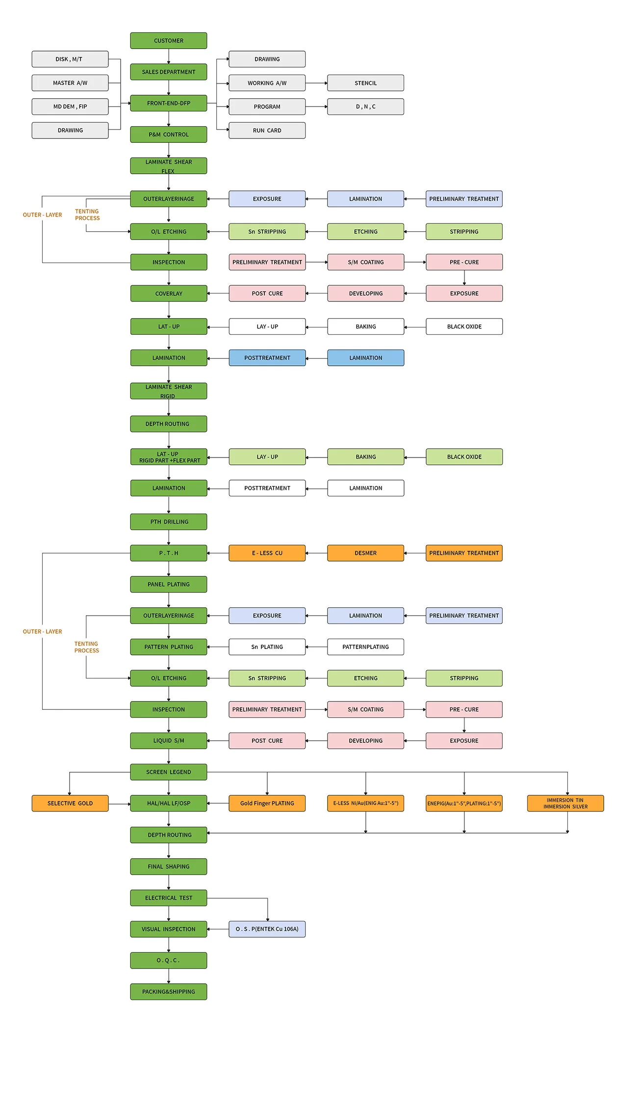
Rigid-Flex PCB Manufacturing Process is a combination of rigid and flexible PCB manufacturing processes. It combines the advantages of both rigid and flexible PCBs, providing superior electrical performance, superior mechanical performance, and superior design flexibility.
The process of Rigid-Flex PCB
The process starts with the design stage where the board is designed to meet the customer’s requirements. The next step is the fabrication process which involves cutting and drilling the PCB to the desired shape and size. After this, the components are soldered onto the board and the board is then laminated with a flexible material. The final step involves testing the board and the individual components, to ensure they are all working correctly. The process is complete when the Rigid-Flex PCB is ready to be used in the customer’s application.
Are you onthe lookout for a good memory foam mattress that combines comfort and quality?
Our rigid-flex PCB capabilities offer numerous advantages for our customers. These include improved space savings, reducing the number of connectors, and improved reliability. Our rigid-flex PCBs are highly flexible and can be bent and folded to fit into tight spaces, allowing for a more compact design. Our PCBs are also more reliable than traditional PCBs, as they can handle more strain and vibration. We also offer improved routing capabilities, allowing for a reduction in the number of connectors needed. This can reduce costs and improve the overall performance of the product. In addition, our rigid-flex PCBs are highly durable, providing long-lasting performance. Our PCBs also offer superior electrical performance, which can result in better data speeds. Lastly, our rigid-flex PCBs are highly customizable, allowing for faster turnaround times and improved cost-effectiveness.
Double-layer Process

Multilayer Process


