HDI PCB Capabilities
Items | Standard | Advanced | Remarks |
Number of Layers | 4-16layer | 3-24L | For orders above 24 layers, please contact our sales rep. |
Material | FR-4 | Rogers/Teflon | For example: |
Maximum PCB Size | 500*500 | 530*800mm | For any sizes beyond this dimension, please contact the sales rep. |
Board Size Tolerance | ±0.13mm | +/-0.1mm for CNC routing | ±0.1mm for CNC routing, and ±0.15mm for V-scoring. |
Board Thickness | 0.8-3mm | 0.6-4mm | Exceed 0.6-4mm, please contact us if your board exceeds these. |
Board Thickness | ±10% | +/-8% | Normally “+ Tolerance” will occur due to PCB processing steps such as electroless copper, solder mask and other types of finish on the surface. |
Board Thickness | ±0.1mm | +/-0.05mm | |
Min Trace | 3.5mil | 3mil | Min manufacturable trace is 3mil(0.075mm), strongly suggest designing trace above 3.5mil(0.09mm) to save cost. |
Min Spacing | 3.5mil | 3mil | Min manufacturable spacing is 3mil(0.075mm), strongly suggest designing spacing above 3.5mil(0.09mm) to save cost. |
Outer Layer Copper Thickness | 1oz |
| Also known as copper weight. 35μm=1oz. Please view the below "Standard PCB" or contact us if you need copper weight greater than 1oz. |
Inner Layer Copper Thickness | 1-4oz | 1-4oz | Inner copper weight as per customer’s request for 4 and 6 layers(Multi-layer laminated structure). Please contact us if you need copper weight greater than 1oz. |
Drill Sizes (CNC) | 0.2-6.0MM | 0.15-6.5MM | Min drill size is 0.15mm, max drill is 6.5mm. Any holes greater than 6.5mm or smaller than 0.3mm will be subject to extra charges. |
Min Width of Annular Ring | 0.15mm | 0.1mm | For pads with vias in the middle, Min width for Annular Ring is 0.1mm(4mil). |
Finished Hole Diameter (CNC) | 0.2-6.0mm | 0.15-6.5mm | The finished hole diameter will be smaller than size of the drill bits because of the copper plating in the hole barrels |
Finished Hole Size Tolerance(CNC) | ±0.076mm | +/-0.05mm | min±0.05mm |
Solder Mask(type) | LPI |
| Liquid Photo-Imageable is mostly adopted. Thermosetting Ink is used in inexpensive paper-based boards. |
Minimum Character Width(Legend) | 0.2mm | 0.12mm | Characters less than 0.12mm wide will be too narrow to be identifiable. |
Minimum Character Height (Legend) | 0.8mm | 0.71mm | Characters less than 0.71mm high will be too small to be recognizable. |
Character Width to Height Ratio (Legend) | 4:1 | 5:1 | In PCB silkscreen legends processing, 1:5 is the most suitable ratio |
Minimum Diameter of Plated Half Holes | 0.5mm | 0.45mm | Design Half-Holes greater than 0.5mm to ensure a better connection between boards. |
Surface Finishing | HASL(1-40um) |
| The most popular three types of PCB surface finish. |
Solder Mask(color) | White, Black, yellow,green,blue, grey, red, purple, and matt color |
| The most popular four colors of PCB solder mask. |
Silkscreen(color) | White, Black, yellow,green,blue, grey,red,purple |
| The most popular two colors of PCB solder mask. |
Panelization | V-scoring, Tab-routing, Tab-routing with Perforation (Stamp Holes) |
| Leave min clearance of 1.0mm between boards for break-routing. For V-score penalization, set the space between boards to zero. |
Others | Fly Probe Testing A.O.I. , E-testing |
|
|
Qualification | UL Certified ISO9001/ISO13485/TS16949; Reach RoHS, IPC, PPAP, IMDS |
|
Overview
HDI PCBs are constructed using advanced fabrication techniques, and are typically composed of multiple layers of material. These layers are bonded together and etched to form the desired circuit paths. The surface finish of HDI PCBs can also be customized to meet the needs of the application, allowing for improved protection against corrosion and other environmental factors.
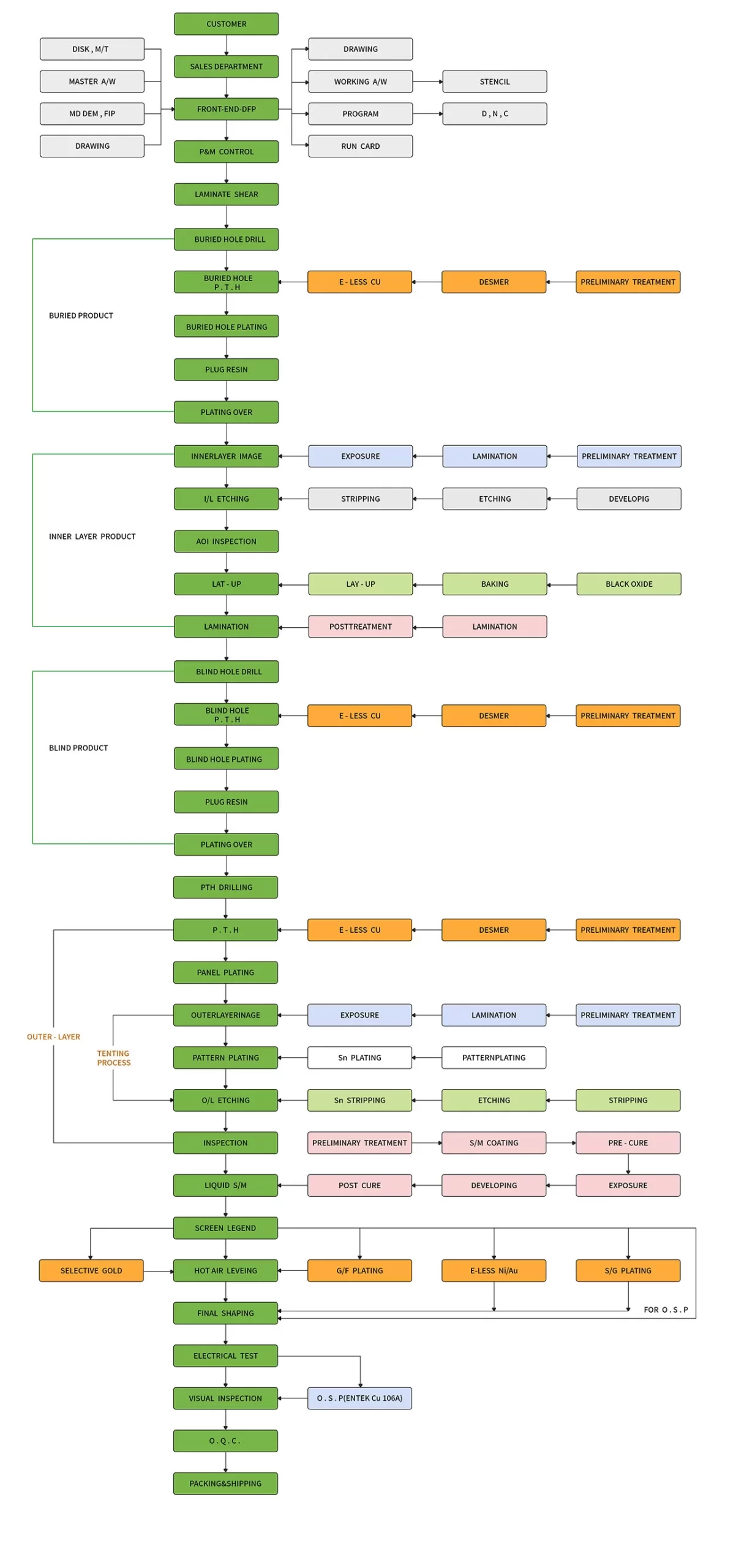
The Process of Manufacturing HDI PCB
HDI PCB manufacturing process involves multiple etching steps to create ultra-thin and ultra-dense circuit boards. It usually uses a combination of laser ablation, chemical etching, and mechanical drilling to create the desired layout. Laser ablation is used to selectively remove copper from the board to create the desired pattern. Chemical etching is then used to create fine routing lines between the components. The mechanical drilling process is then used to create the vias, which are tiny holes that help to connect the layers of the board. Finally, the solder mask is added to protect the board from oxidation and to make it easier to solder components to the board.
Advantages of Our HDI PCB Capabilities
Our HDI PCB capabilities offer many advantages including reduced board size and weight, increased wiring density and shorter trace lengths, increased circuit density and flexibility, improved electrical performance, improved thermal performance, and improved signal integrity. Our HDI PCBs also have higher reliability and improved manufacturability due to the use of finer lines and spaces, improved material processes, and increased trace and via count. In addition, our HDI PCBs are also more cost-effective than traditional PCBs, as they require fewer layers and components, resulting in less material and labor costs. Finally, our HDI PCBs are more environmentally friendly due to the use of recycled materials and reduced energy consumption.
HDI PCB Process


