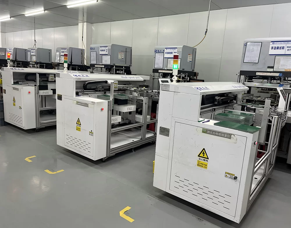
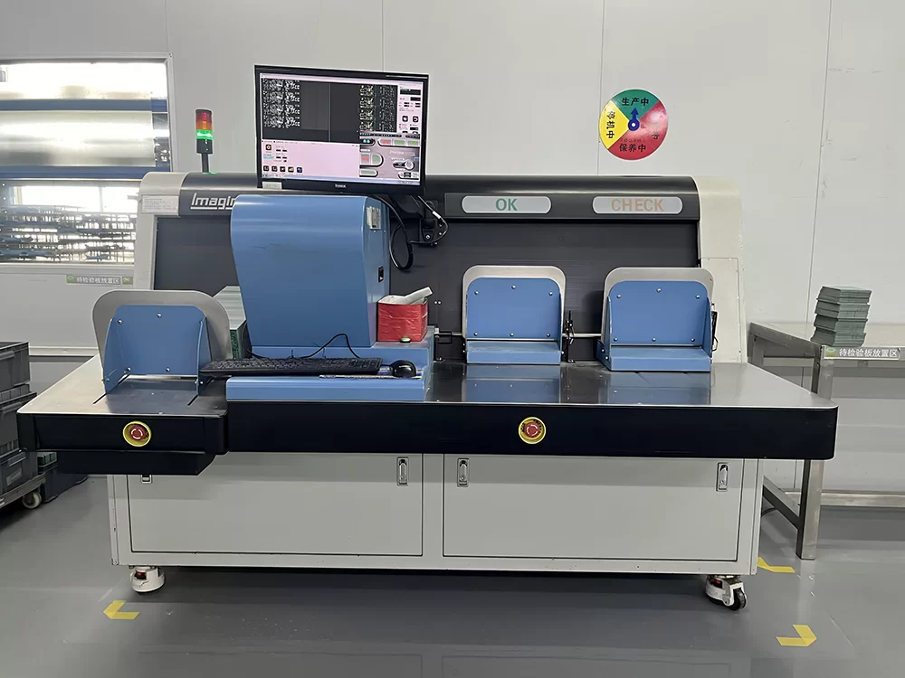
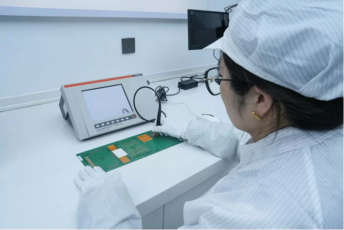
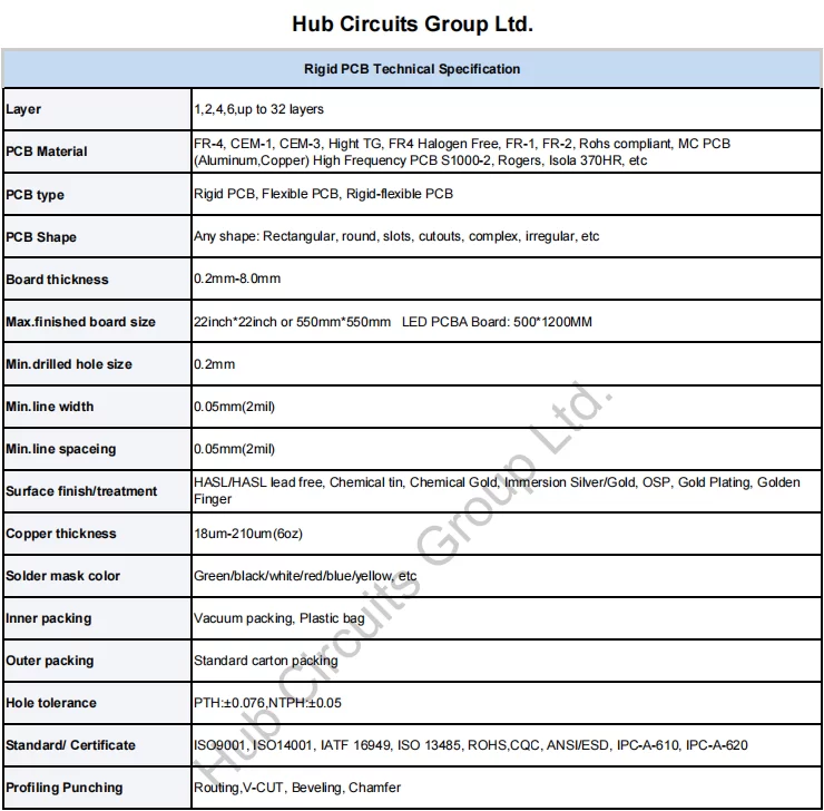
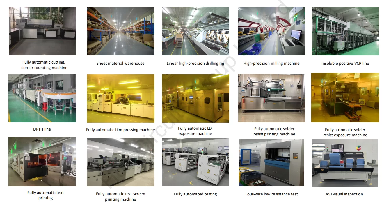
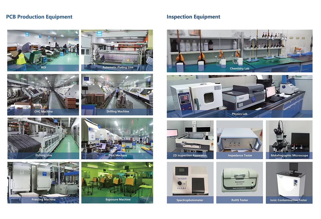
General PCB Manufacturing Process Flow:
1: PCB Design and File Preparation
2: Photoplotting and Film Production
3: Inner Layer Imaging and Etching
4: Layer Alignment and Lamination
5: Drilling
6: Chemical Copper Deposition
7: Outer Layer Imaging and Electroplating
8: Outer Layer Etching
9: Solder Mask Application
10: Silkscreen Printing
11: Surface Finishing
12: Electrical Testing
13: Routing and V-Scoring
14: Final Inspection, Packaging, and Shipping
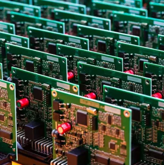
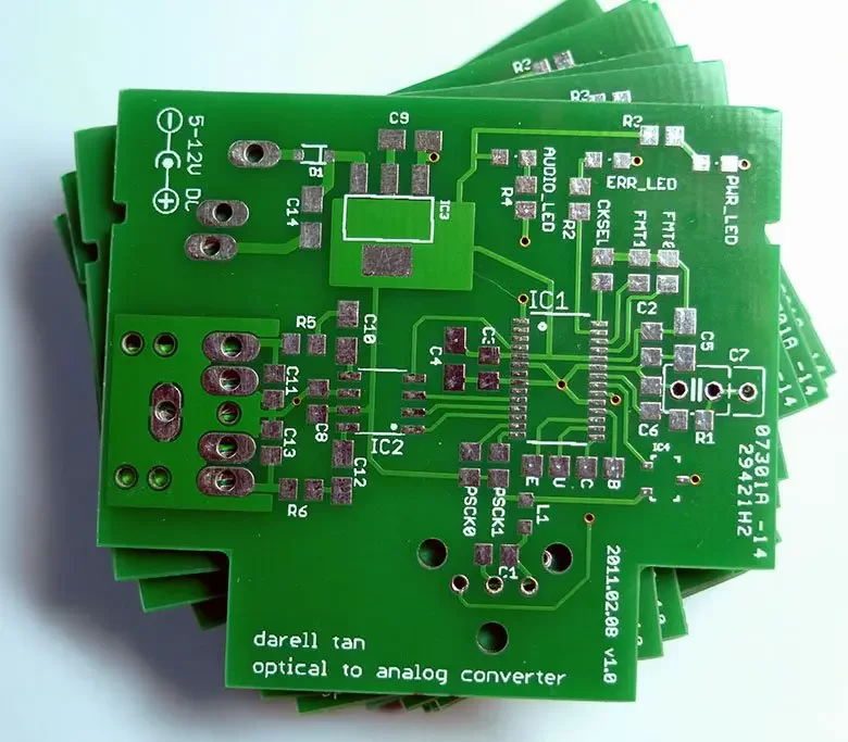
The PCB we made:
E-Test File Requirements
For accurate and complete testing, we recommend customers provide a netlist file (IPC-356 format) along with Gerber data. A netlist derived directly from the design source ensures high fidelity and accurate fault detection. If a netlist is not provided, we will generate one from the Gerber files for continuity testing.
Providing the design netlist:
Increases test coverage accuracy
Avoids discrepancies from CAM changes
Ensures compliance with high-reliability standards
FR-4 PCB
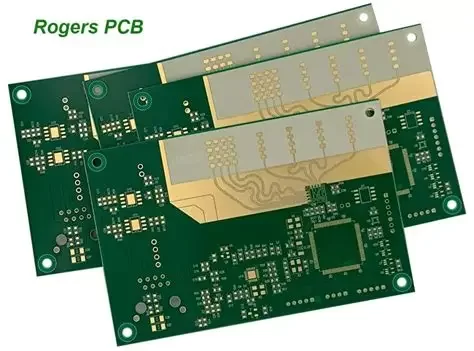
Rogers PCB
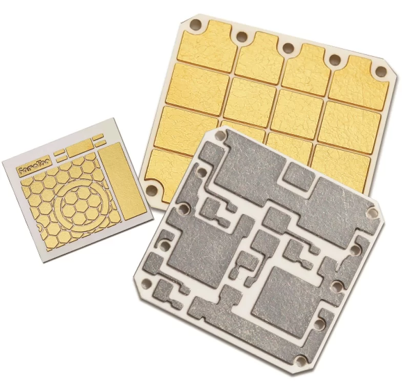
Ceramic PCB
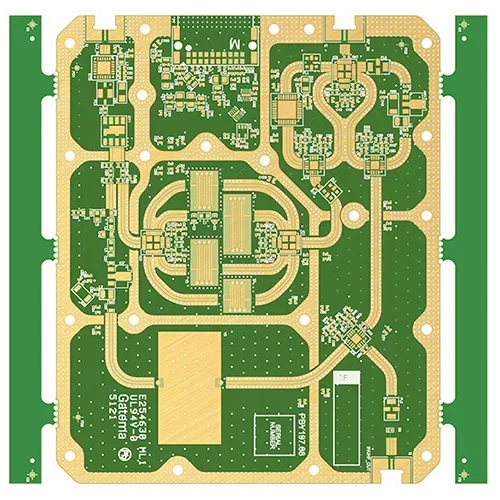
High frequency PCB

IC Substrate PCB
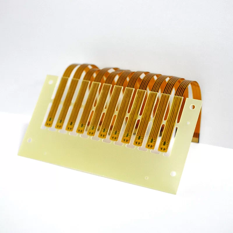
Rigid Flex PCB

HDI Portable Electron PCB
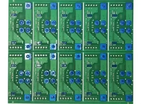
Blue Peelable PCB
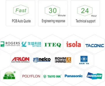
Our PCB material

