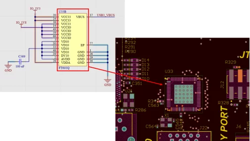
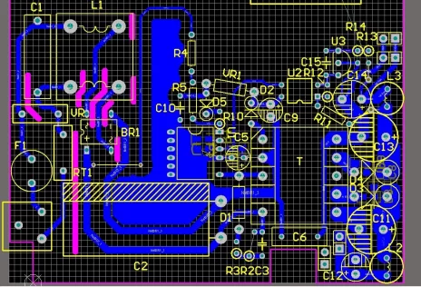
PCB reverse
PCB reverse engineering involves using reverse engineering techniques to analyze an existing circuit board. This process involves replicating the original electronic product's PCB files, Bill of Materials (BOM), schematic diagram, and PCB silkscreen production files in a 1:1 ratio. Then, based on these files, PCB fabrication, component soldering, flying probe testing, and circuit board debugging are performed to completely replicate the original electronic product's circuit board prototype. It is also known as circuit board copying, PCB cloning, or PCB reverse design.

Reverse steps
1. Record PCB board components
When you get a PCB, first write down the model number, parameters, and location of all components on paper, especially the orientation of diodes, transistors, and IC notches. It's best to take two photos of the component locations with a digital camera. Modern PCBs are becoming increasingly sophisticated; some diodes and transistors are practically invisible if you're not paying close attention.
2. Scanned images of disassembled components
Remove all components and remove the solder from the PAD holes. Clean the PCB with alcohol, then place it in the scanner. When scanning, slightly increase the scanning resolution to obtain a clearer image. Next, lightly sand the top and bottom layers with wet sandpaper until the copper film shines. Place it in the scanner, launch Photoshop, and scan both layers separately in color. Note that the PCB must be placed horizontally and vertically in the scanner; otherwise, the scanned image will be unusable.
3. Adjust the scanned image
Adjust the contrast and brightness of the canvas to create a strong contrast between the areas with and without the copper foil. Then convert the image to black and white and check the lines for clarity. If they are not clear, repeat this step. If clear, save the image as a black and white BMP file (TOP BMP and BOT BMP). If any problems are found, you can use Photoshop to repair and correct them.
4. Importing images into the reverse engineering software
Convert both BMP files to PROTEL format. Import the two layers into PROTEL. If the positions of the PADs and VIAs on both layers are roughly aligned, the previous steps were successful. If there are discrepancies, repeat step three. Therefore, PCB reverse engineering is a task that requires extreme patience, as even small problems can affect the quality and the degree of compatibility after reverse engineering.
5. Convert image to PCB file
Convert the TOP layer BMP to a TOP PCB, making sure to convert it to the SILK layer (the yellow layer). Then, trace the outlines on the TOP layer and place the components according to the schematic from step two. After finishing, delete the SILK layer. Repeat this process until all layers are drawn.
6. PCB file inspection and adjustment
Simply import the TOP PCB and BOT PCB into PROTEL and combine them into one diagram.
7. Compare with the original board to check and make modifications.
Use a laser printer to print the TOP LAYER and BOTTOM LAYER onto transparent film (1:1 scale). Place the film onto the PCB, check and make corrections as needed, then test to verify that the copied electronic performance matches the original board. Passing the test indicates successful copying.

Advantages of Reverse
1. Advanced equipment and a professional team
The company has purchased multiple advanced PCB reverse engineering machines, circuit board testing instruments, and the latest reverse engineering software, and has cultivated a team of experienced senior technicians. We can test all states of PCB circuit signals, ensuring that the PCB clone board is 100% identical to the original board, meeting your reverse engineering requirements.
2. Better prices and better service
Hubcircuits Group offers transparent and open pricing for reverse engineering, with no unnecessary or arbitrary fees. We sign project contracts to guarantee the successful completion of clients' reverse engineering projects. Dedicated customer service personnel liaise with clients, promptly relaying client requirements to the reverse engineering engineers and providing timely updates on the progress.
3. Reasonable delivery time and comprehensive after-sales service.
The PCB reverse engineering cycle is crucial to a product's market sales. Most single-sided and double-sided reverse engineering can be completed within 1-2 days. PCB reverse engineering for general consumer electronics products takes only 2-4 days, while PCB reverse engineering for computer motherboards takes 4-6 days. For rapid prototyping, double-sided boards can be delivered within 24 hours, and four-layer boards within 48 hours.
4. Complete business operations and excellent distribution channels
We have a professional OEM/PCB manufacturing plant, equipped with advanced foreign equipment and technology, to provide processing and production services for your samples. We can offer PCB reverse engineering, chip decryption, component procurement services, through-hole and surface mount (DIP, SMD/SMT) soldering, PCBA manufacturing and material supply-one-stop service.
PCB board reading business process
Refers to the entire process of the customer's board copying service, including but not limited to the following steps:
1. Project consultation/quotation PCB copying cost
Customers provide their own board printing needs, board type introduction, board printing time period expectations and related PCB board known information, and communicate with the board copying company's service or technical personnel to negotiate the board copying price.
2. The customer provides the motherboard and pays the deposit in advance
If the PCB board is sent by express, please pay attention to wrapping it to avoid damage.
3. The company reads the board according to customer needs
4. Please confirm the completion of the copying
5. Confirm the completion and settle the final payment
PCB board reversing process
PCB is a printed circuit board without components, while a printed circuit board with components is called PCBA. The following is the PCB board reading process with components.
1. Scan the board picture
Note: Since there may be small patch elements under the large components, you can scan them first, then remove the large ones and scan them again.
2. Dismantling the board
Remove all components and remove the tin from the PAD holes. Clean the PCB with washing water, then put it into the scanner, the scanner scans according to the precision of the board to select the appropriate pixels, so as to get a clearer image, start OHTOSHOP, scan the silk screen surface in color, save the file and print it out for later use;
Note: When dismantling the plate, pay attention to the polarity and orientation of the components.
3. Make a BOM sheet
Refer to the circuit board picture in the first step, record the model, parameters, and position of all the element components on paper, especially the diode, the direction of the three tubes, the direction of the IC notch, etc., and finally make a BOM table;
4. Grinding plate
Lightly polish the two layers of TOP LAYER and BOTTOM LAYER with water gauze paper, polish until the copper film shines, put it into the scanner, start PHOTOSHOP, and sweep the two layers in color respectively.
5. Adjust the contrast and brightness of the canvas to make the part with copper film and the part without copper film contrast strongly, then turn the second picture to black and white, check whether the lines are clear, if not, repeat this step. If it is clear, save the image as a black and white BMP format file TOP.BMP and BOT.BMP, and if you find a problem with the drawing, you can also use PHOTOSHOP to repair and correct it.
6. Start the PCB board reading software Protel, load the scanned PCB board picture in the file menu, convert the two BMP format files into PROTEL format files respectively, and transfer the two layers in PROTEL, such as the positions of PAD and VIA over the two layers basically coincide, indicating that the first few steps are done well, if there is a deviation, repeat step 4.
7. Convert the BMP of the TOP layer into TOP.PCB, pay attention to convert it to the SILK layer, and then you can trace the line in the TOP layer, and place the device according to the drawing in the second step. Delete the SILK layer after drawing.
- 8. Convert the BMP of the BOT layer to BOT.PCB, the same as above, convert it to the SILK layer, and then you can trace the line in the BOT layer. Delete the SILK layer after drawing.
- 9. Call in TOP.PCB and BOT.PCB in PROTEL and combine them into one diagram.
- 10. Use a laser printer to print the TOP LAYER and BOTTOM LAYER onto the transparencies (1:1 ratio), put the film on the PCB, compare whether there is a mistake, if it is correct, a simple double-sided board is made!


