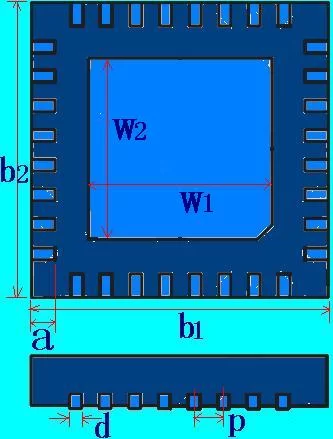
PCB Solder Pad Design Standard - Solder Pad Specification Size (Second)
During stackup design, it is recommended to set the center layer to the maximum copper thickness and further balance the remaining layers to match their mirrored opposite layers.
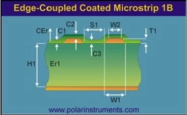
To determine the requirements of impedance control, to standardize the impedance calculation method, to formulate the guidelines of impedance test COUPON design, and to ensure that the products can meet the needs of production and customer requirements.
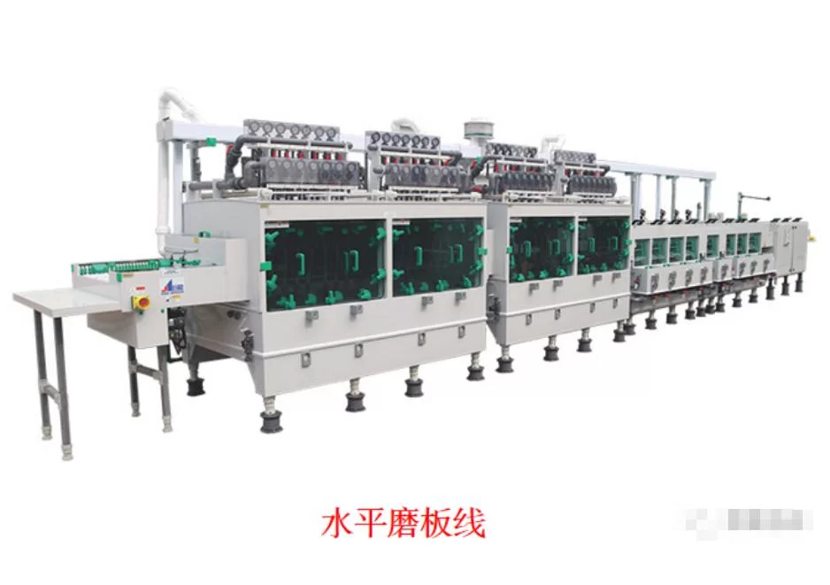
Deposit a thin layer of copper on the entire printed circuit board (especially on the hole wall) for subsequent hole plating, to make the hole metalized (with copper inside for conductivity), and achieve interlayer conductance.
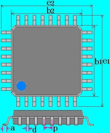
Component type + size system + appearance size specifications named.
With the advancement of high integration and assembly (especially chip-scale/µ-BGA packaging) technology of electronic components (groups).
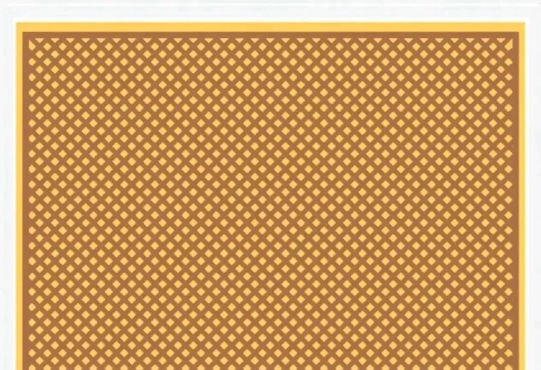
MARK point: This type of point is used to automatically locate the position of the PCB board in SMT production equipment, and must be designed when designing PCB boards.
Copper-clad PCB mainly plays three roles in the entire printed circuit board: conduction, insulation, and support.
The physical parameters that need to be studied include anode type, anode-cathode spacing, current density, agitation, temperature, rectifier, and waveform.
The design of electronic products is from drawing schematic diagrams to PCB layout and wiring.
PCB stands for Printed Circuit Board. It is a thin board made of insulating material, usually fiberglass or plastic, with conductive pathways or tracks printed onto it.
Quantity: minimum of 2, suggested 3, with additional Local Mark for boards over 250mm or with Fine Pitch components (non-chip components with pin or solder spacing less than 0.5mm).
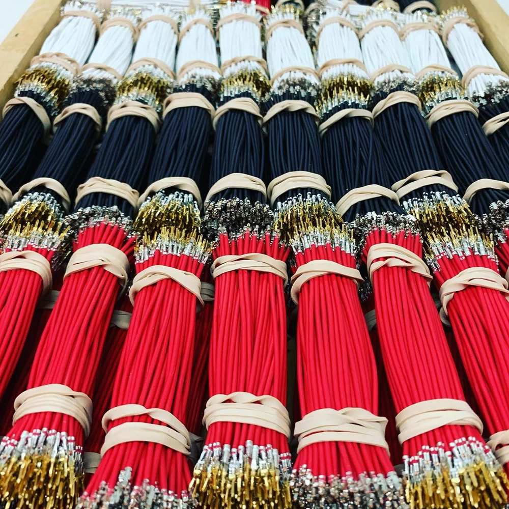
Managing kitting and packaging in-house can be time-consuming, costly, and error-prone.
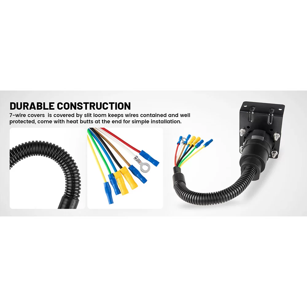
Maybe an off-the-shelf cable can't meet your needs.
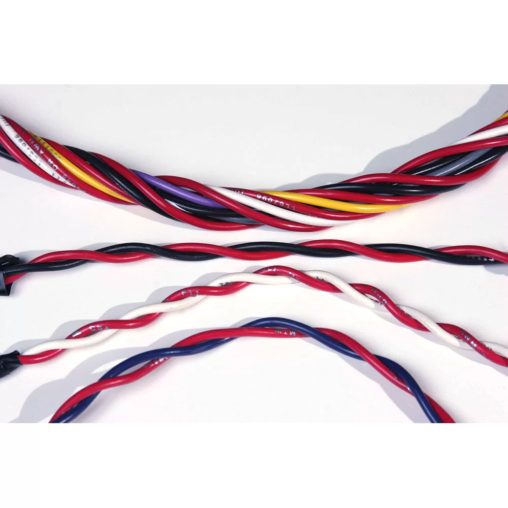
Twisting entwines multiple wires and arranges them tightly next to each other. Depending on the AWG size, we can group up to fifty conductors.
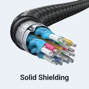
Shielding refers to the metallic layer surrounding a cable’s conductor, created to limit signal interference between the wire and external fields.

