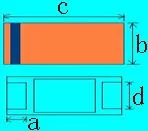
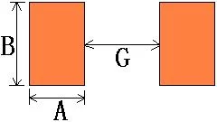
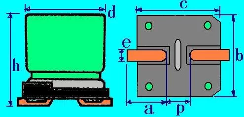
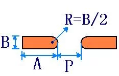
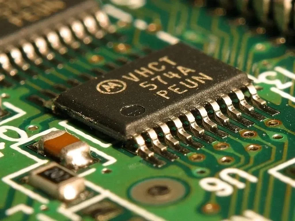
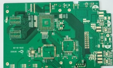
Note: The following design standards refer to the IPC-SM-782A standard and the design of some famous Japanese design manufacturers and some better design solutions accumulated in the manufacturing experience. For your reference and use (the general idea of pad design: CHIP pieces of standard size, according to the size specifications to give a pad design standards; size is not standard, according to its material number to give a pad design standards. IC, connector components in accordance with the material number or specifications grouped to give a design standard.) To reduce design problems to the actual production of many problems.
Specifications (or material number): 0201 (0603)
Material specific parameters (mm):

a=0.10±0.05,b=0.30±0.05,c=0.60±0.05
Pad design (mm):
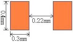
Note: Applicable and common resistors, capacitors, inductors
Specifications (or material number): 0402 (1005)
Material specific parameters (mm):

a=0.20±0.10,b=0.50±0.10,c=1.00±0.10
Pad design (mm):

Printed tin stencil design: centered on the center of the pad, openings round D = 0.55mm
Stencil design: opening width 0.2mm (stencil thickness T recommended thickness of 0.15mm)
Note: Applicable and common resistors, capacitors, inductors
Specification (or material number): 0603 (1608)
Material specific parameters (mm):

a=0.30±0.20,b=0.80±0.15,c=1.60±0.15
Pad design (mm)
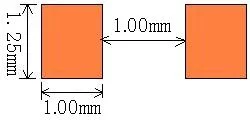
Note: Applicable and common resistors, capacitors, inductors
Specifications (or material number): 0805(2012)
Material specific parameters (mm)

a=0.40±0.20,b=1.25±0.15,c=2.00±0.20
Pad design (mm)

Note: Applicable and common resistors, capacitors, inductors
Specification (or material number): 1206 (3216)
Material specific parameters (mm)

a=0.50±0.20,b=1.60±0.15,c=3.20±0.20
Pad design (mm)
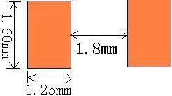
Note: Applicable and common resistors, capacitors, inductors
Specification (or material number): 1210(3225)
Material specific parameters (mm)

a=0.50±0.20,b=2.50±0.20,c=3.20±0.20
Pad design (mm)

Note: Applicable and common resistors, capacitors, inductors
Specification (or material number): 1812(4532)
Material specific parameters (mm)

a=0.50±0.20,b=3.20±0.20,c=4.50±0.20
Pad design (mm)
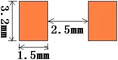
Note: Applicable and common resistors, capacitors, inductors
Specification (or material number): 2010(5025)
Material specific parameters (mm)

a=0.60±0.20,b=3.20±0.20,c=6.40±0.20
Pad design (mm)
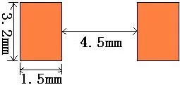
Note: Applicable and common resistors, capacitors, inductors
Specification (or material number): 2512(6432)
Material specific parameters (mm)

a=0.60±0.20,b=3.20±0.20,c=6.40±0.20
Pad design (mm)

Note: Applicable and common resistors, capacitors, inductors
Specification (or material number): 5700-250AA2-0300
Material specific parameters (mm)
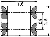
Pad design (mm)
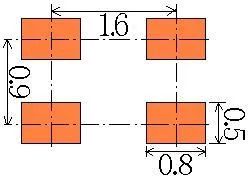
Printed tin stencil design: 1:1 opening, not to avoid tin beads
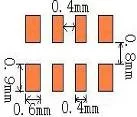
Specification (or material number): Drain resistance 0404 (1010)
Material specific parameters (mm)
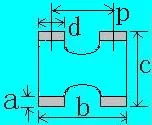
a=0.25±0.10,b=1.00±0.10,c=1.00±0.10,d=0.35±0.10,p=0.65±0.05
Pad design (mm)
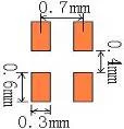
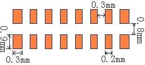
Specification (or material number): Drain resistance 1206(3216)
Material specific parameters (mm)
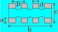
a=0.30±0.15,b=3.2±0.15
c=1.60±0.15,d=0.50±0.15
p=0.80±0.10
Pad design (mm)
Specification (or material number): Drain resistance 1606(4016)
Material specific parameters (mm)

a=0.25±0.10,b=4.00±0.20
c=1.60±0.15,d=0.30±0.10
p=0.50±0.05
Pad design (mm)
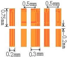
Specification (or material number): 472X-R05240-10
Material specific parameters (mm)
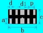
a=0.38±0.05,b=2.50±0.10
c=1.00±0.10,d=0.20±0.05
d1=0.40±0.05,p=0.50
Pad design (mm)
Tantalum capacitors
Specification (or material number) | Material specific parameters (mm): | Pad design (mm): |
2312 | a=1.30±0.30,b=3.20±0.30 | A=2.00,B=2.20,G=3.20 |
2917 | a=1.30±0.30,b=4.30±0.30 | A=2.00,B=2.40,G=4.50 |
1206 | a=0.80±0.30,b=1.60±0.20 | A=1.50,B=1.20,G=1.40 |
1411 | a=0.80±0.30,b=2.80±0.20 | A=1.50,B=2.20,G=1.70 |
Aluminum electrolytic capacitors
Material specific parameters (mm):
| Pad design (mm):
| |
(Ø4×5.4) | a=1.8±0.2,b=4.3±0.2 | A=2.40,B=1.00 |
(Ø5×5.4) | a=2.2±0.2,b=5.3±0.2 | A=2.80,B=1.00 |
(Ø6.3×5.4) | a=2.6±0.2,b=6.6±0.2 | A=3.20,B=1.00 |
(Ø6.3×7.7) | a=2.6±0.2,b=6.6±0.2 | A=3.20,B=1.00 |
(Ø8.0×6.5) | a=3.0±0.2,b=8.3±0.2 | A=3.20,B=1.00 |
(Ø8×10.5) | a=3.0±0.2,b=8.3±0.2 | A=3.60,B=1.30 |
(Ø10×10.5) | a=3.5±0.2,b=10.3±0.2 | A=4.20,B=1.30 |

