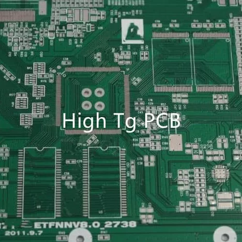
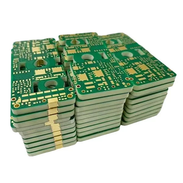
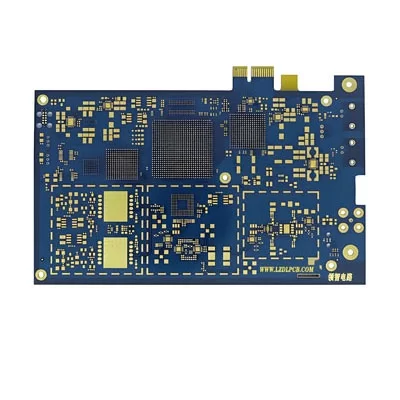
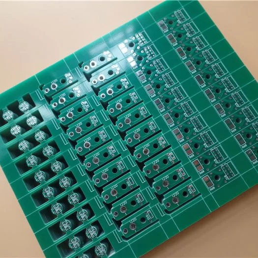
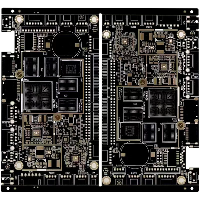
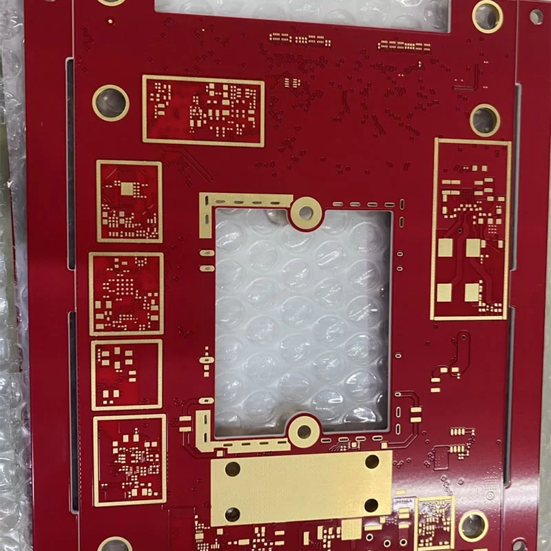
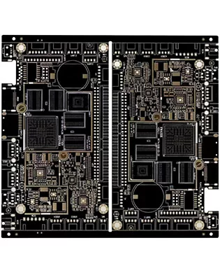
Mobile Phone HDI PCB
Data Sheet
Model: Mobile Phone HDI PCB
Layer: 8
- Material: TG170 FR4
- Finished Board Thickness:1.0mm
- Finished Copper Thickness:loz
- Min Line Width/space:23mil(0.075mm)
- Min Hole:24mil(0.1mm)
- Surface Finish:ENIG
- Solder Mask Color:Green
- Legend Color:Black
- Application:Consumer Electronics
Considerations for the layered structure in HDI design
Layer Count Planning
The layer count is determined by signal density and complexity. Typically, 8–12 layers are used, with cores and outer layers connected via blind and buried vias.
- Material SelectionSelect high-frequency materials with low dielectric constant (Dk) and low loss factor (Df) (e.g., FR4, Rogers) to ensure signal integrity.
- Blind and Buried Via Design① Blind Via: Connects outer and inner layers. Its depth must not exceed the board thickness, and the hole diameter is controlled (typically 4–6 mils).② Buried Via: Enables interconnection between inner layers, avoiding surface space occupation. Processing must be completed before inner layer lamination.
- Lamination SymmetryMaintain symmetric dielectric layer thickness (e.g., consistent PP sheet thickness) to prevent warping.
- Impedance ControlCalculate and control impedance based on the laminate structure to ensure the characteristic impedance of each signal layer meets design requirements.
- Heat Dissipation & Mechanical PerformanceThe laminate structure must meet heat dissipation requirements, with rational distribution of power and ground layers, while ensuring the circuit board’s mechanical strength and flexibility.
Considerations for HDI boards Design
Laser via diameter: 0.076–0.15mm (3–6 mils); annular ring width ≥ 3 mils.
- Laser vias must not be through-hole; dielectric layer thickness ≤ 0.1mm.
- Copper thickness of laser via processing layers and connecting layers ≤ 1oz.
- Lamination design must be symmetrical: finished boards should have an even number of layers, with copper thickness per layer and dielectric layer thickness kept as symmetrical as possible.
Are you onthe lookout for a good memory foam mattress that combines comfort and quality?
Manufacturing HDI boards is nothing like regular PCBs. It’s multi-step, precision-driven, and highly sequential.
Here’s a simplified flow:
1. Inner Layer Imaging & Etching: Inner copper layers are patterned using photolithography.
- 2. Core Lamination: The etched cores are laminated with prepreg and copper foil.
- 3. Laser Drilling (Microvias): Laser drills sub-0.15mm vias through the top layer. UV or CO2 lasers are typically used.
- 4. Desmearing and Hole Cleaning: Plasma cleaning ensures debris-free via holes for reliable plating.
- 5. Electroless Copper Deposition: A thin copper layer is deposited inside microvias for conductivity.
- 6. Electroplating: Additional copper is plated to increase via wall thickness.
- 7. Outer Layer Imaging & Etching: Top signal layers are created. Fine traces are patterned.
- 8. Sequential Lamination: Additional layers are added as needed, repeating steps 3–7 for each HDI cycle.
- 9. Via Fill & Planarization: Via-in-pad structures are filled with epoxy resin and planarized via CNC.
- 10. Solder Mask and Surface Finish: ENIG or OSP surface finishes are applied.
- 11. Final Testing: Finally, electrical tests validate integrity.
If you have any camping barbeque equipment inquiry, please feel free to contact us.
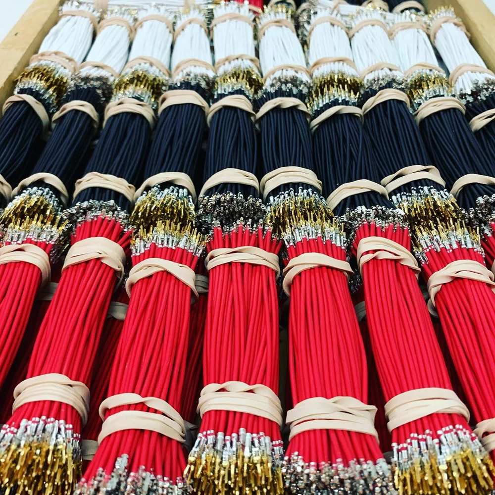
Managing kitting and packaging in-house can be time-consuming, costly, and error-prone.
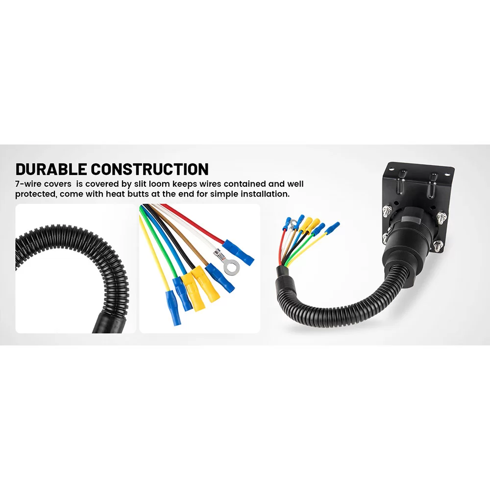
Maybe an off-the-shelf cable can't meet your needs.
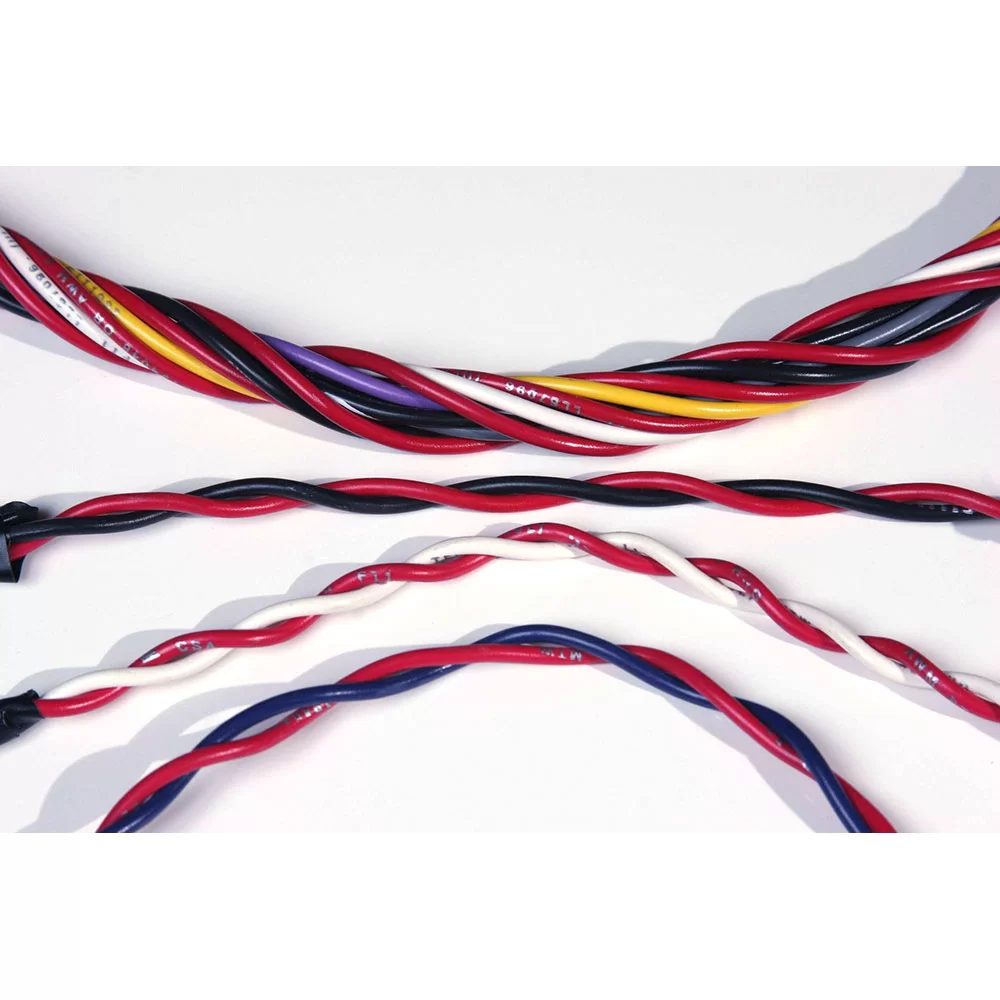
Twisting entwines multiple wires and arranges them tightly next to each other. Depending on the AWG size, we can group up to fifty conductors.
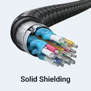
Shielding refers to the metallic layer surrounding a cable’s conductor, created to limit signal interference between the wire and external fields.
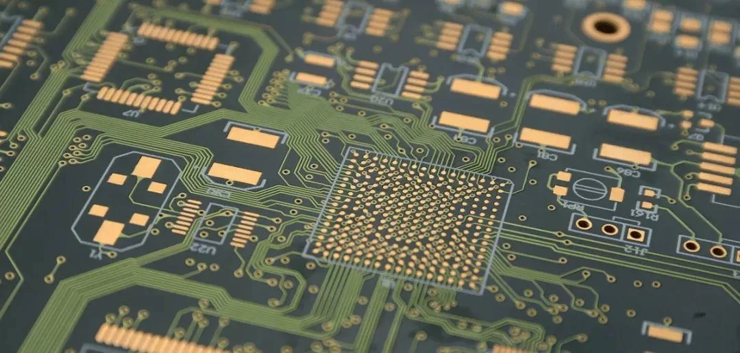
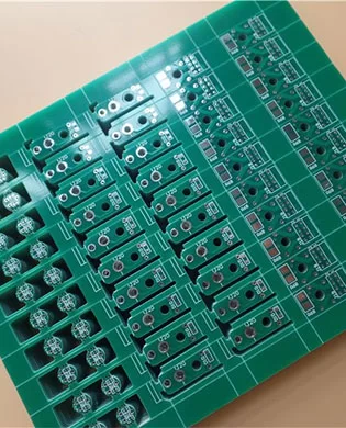
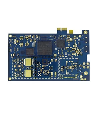
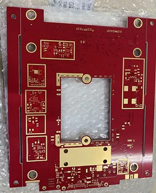
PCB manufacturing is the process of building a physical PCB from a PCB design according to a certain set of specifications.

The following design standards refer to the IPC-SM-782A standard and the design of some famous Japanese design manufacturers and some better design solutions accumulated in the manufacturing experience.
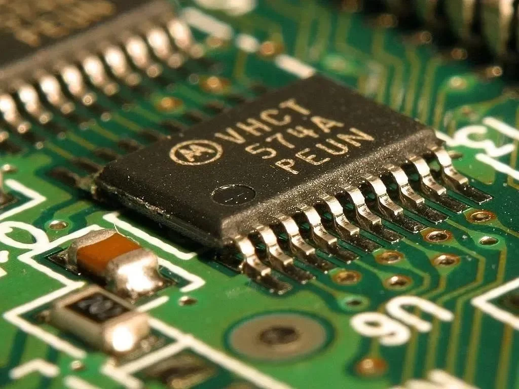
Via holes, also known as through holes, play a role in connecting different parts of a circuit board.

