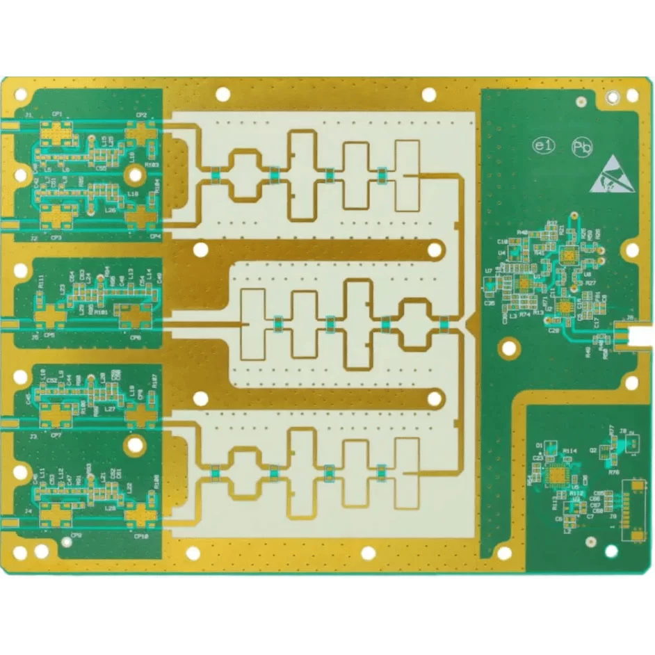
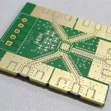
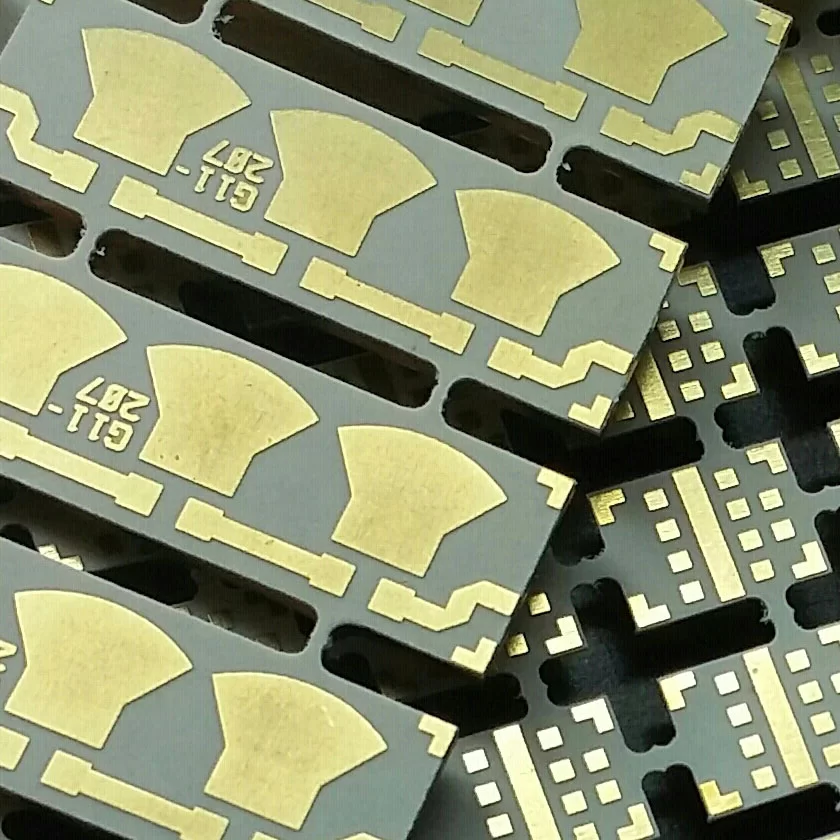
Hybrid Microwave PCB
Data Sheet
Moduel: Hybrid Microwave PCB
Material: FR4+Teflon, Ceramic, Rogers
Quality standard: IPCB6012 Class2
pcb material dielectric constant: 2.2-16
the texture of material: Hybrid pcb, Mixed PCB
Layers: 2layer – multilayer hybrid PCB
Thickness: 0.1mm-12mm
Copper thickness: 0.5oz-30z
Surface technology: Gold, OSP
Application: High-frequency Hybrid Microwave PCB
What‘s Hybrid microwave circuit board?
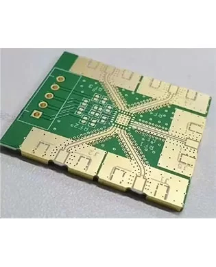
Hybrid microwave PCB is using a dissimilar materials with the intent of optimizing electrical performance and improving system reliability focused towards high-frequency RF applications.
These designs include a combination of FR-4 material and PTFE laminates typically. It allows the designer to condense both RF functionality and RF functionality on the same PCB and reduce both the footprint of the device and the costs.
Manufacturing Innovation
By combining a low-loss material (such as PTFE or Rogers) with another core material (such as FR-4) in a single laminate. Hybrid Microwave PCBs can:
Significantly reduce space and save costs
Integrate RF and non-RF components on a single board
Optimize signal integrity for complex applications
Hybrid RF PCB Laminate Construction Considerations
When manufacturing PCBs with different materials, expertise in laminate physical properties and equipment capabilities is critical. Due to varying CTE values of all material layers (e.g., FR4, PTFE, copper), each expands at a different rate during high-temperature processes like lamination. This causes major registration issues (from differential shrinkage/expansion) and potential delamination at copper-substrate interfaces. So, not all materials suit hybrid applications—some are unmanufacturable even if they meet performance requirements.
Collaborating with supplier early in the design process delivers the best results, as they know which materials pair optimally. For example, Rogers 5880 is an excellent RF material for high-reliability uses. Its key challenge is shrinkage after copper etching, so fabricators must understand this to compensate in their processes.
Applications
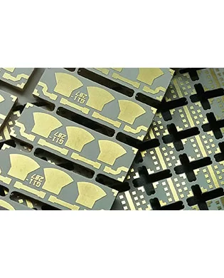
High-frequency Hybrid Microwave PCBs are widely used in wireless antennas, base station receiving antennas, power amplifiers, radar systems, navigation systems and other communication equipment.
If you have any camping barbeque equipment inquiry, please feel free to contact us.
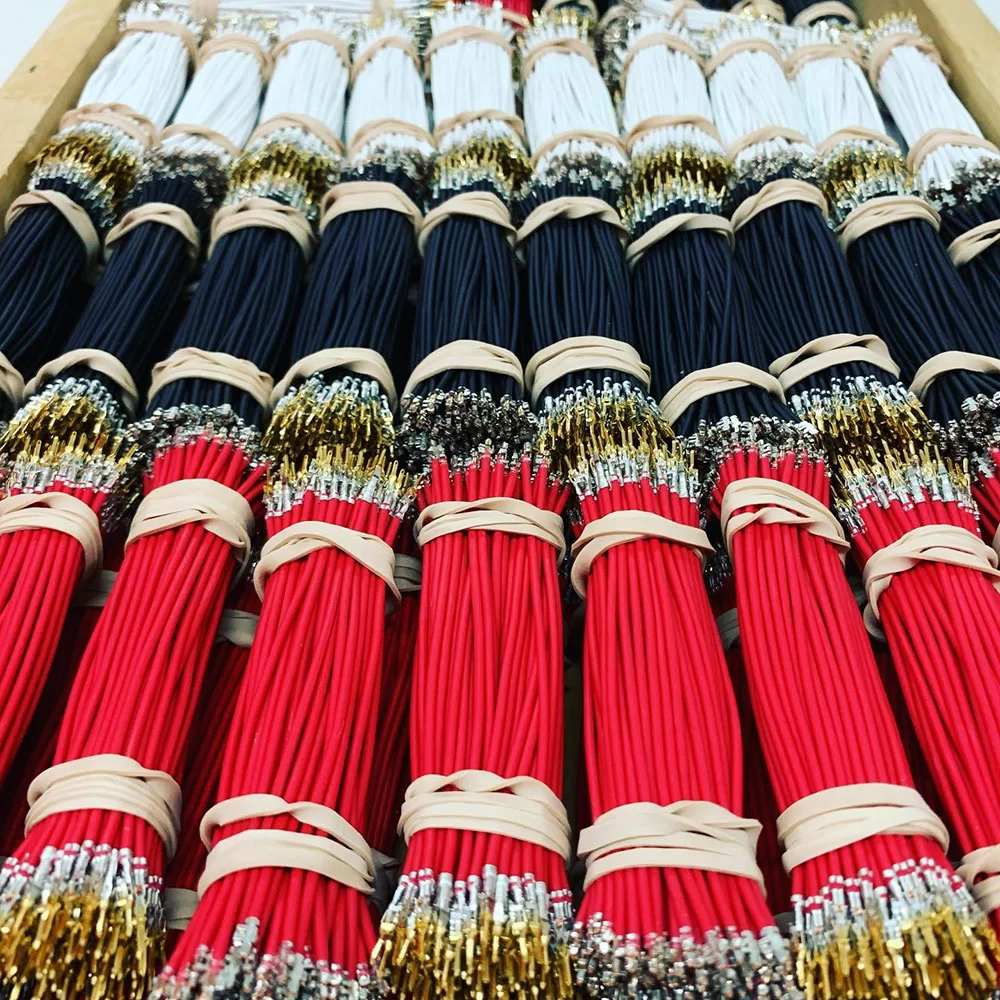
Managing kitting and packaging in-house can be time-consuming, costly, and error-prone.
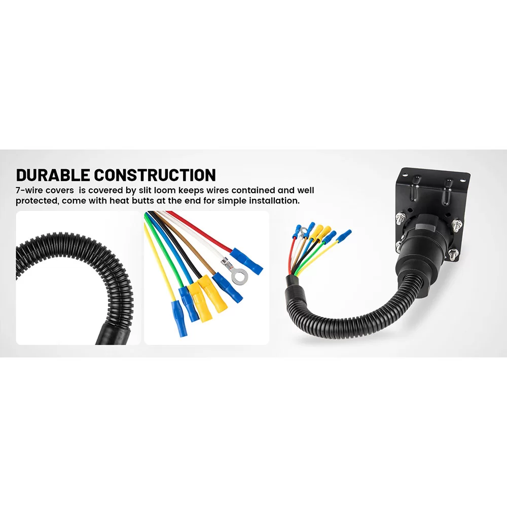
Maybe an off-the-shelf cable can't meet your needs.
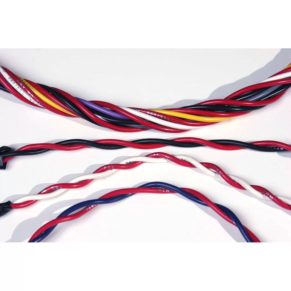
Twisting entwines multiple wires and arranges them tightly next to each other. Depending on the AWG size, we can group up to fifty conductors.
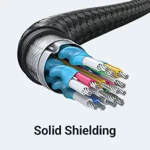
Shielding refers to the metallic layer surrounding a cable’s conductor, created to limit signal interference between the wire and external fields.
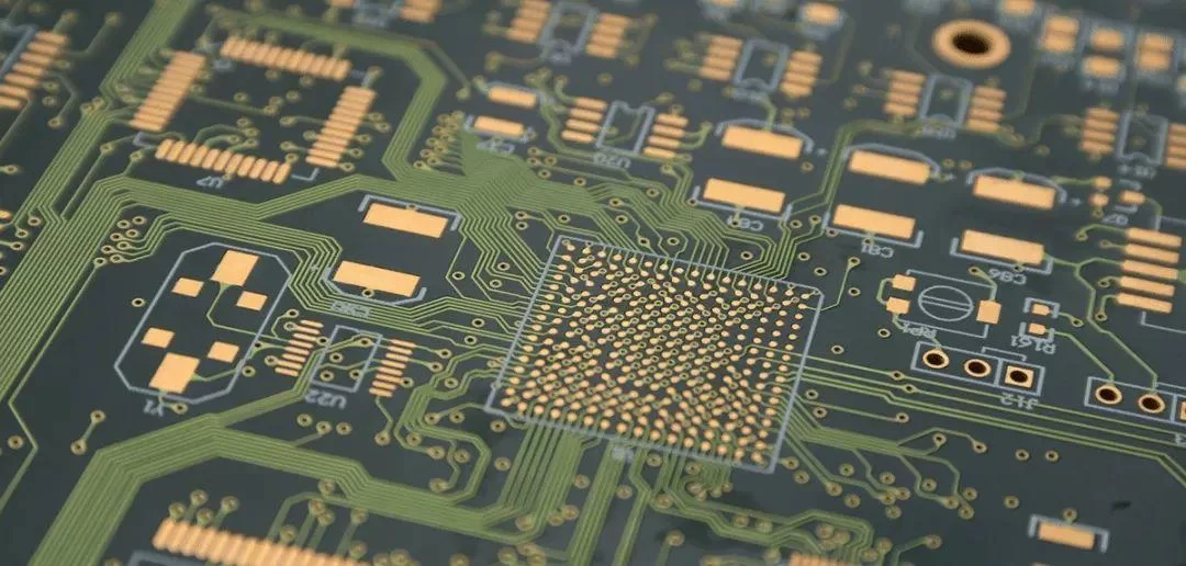
PCB manufacturing is the process of building a physical PCB from a PCB design according to a certain set of specifications.

The following design standards refer to the IPC-SM-782A standard and the design of some famous Japanese design manufacturers and some better design solutions accumulated in the manufacturing experience.
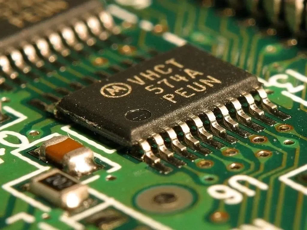
Via holes, also known as through holes, play a role in connecting different parts of a circuit board.

