Golden Finger PCB
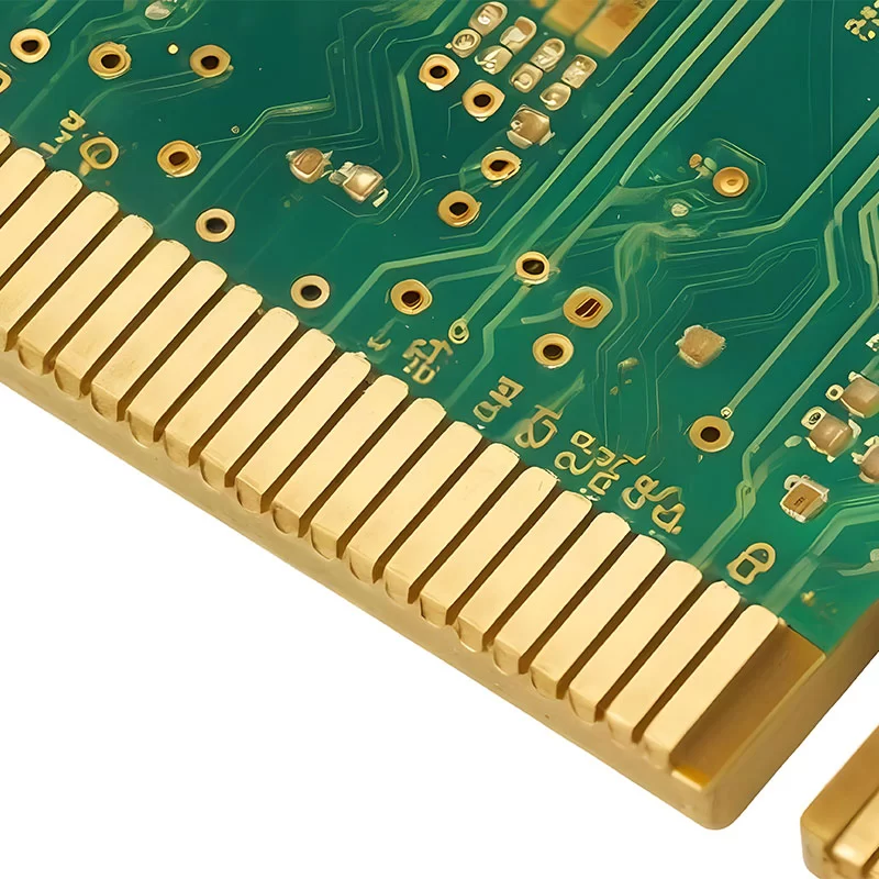
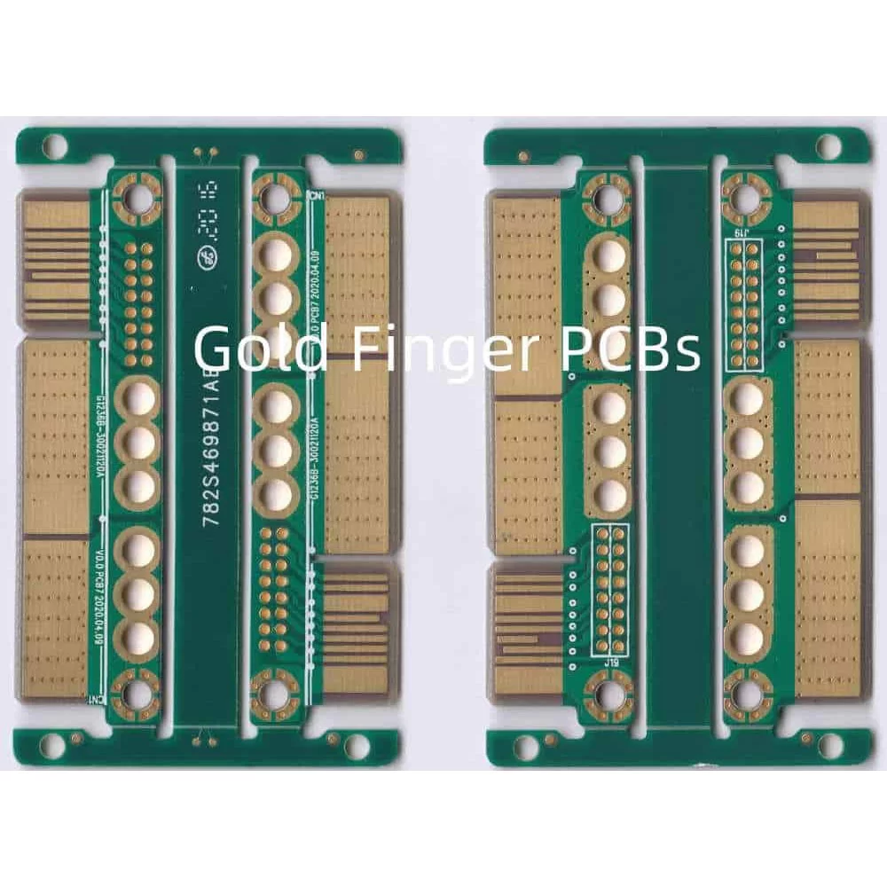
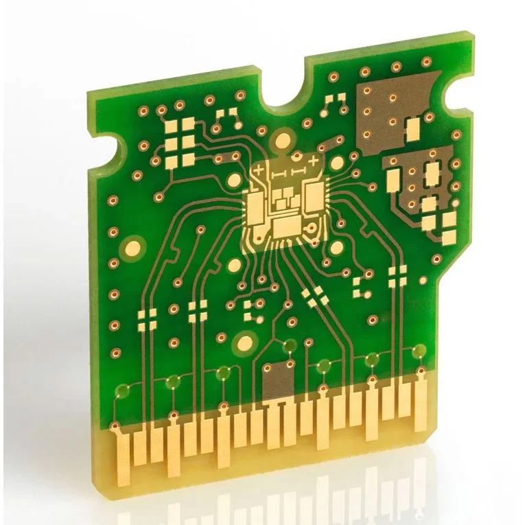
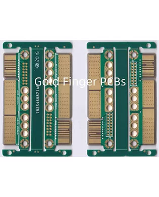
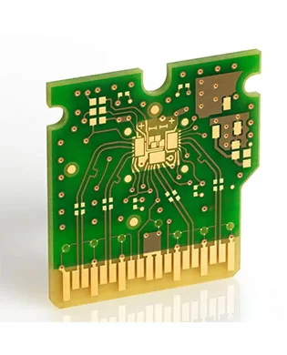
Gold finger PCB is a specialized printed circuit board featuring gold-plated conductive contacts (known as "gold fingers") designed along the board's edge. It is primarily used to achieve reliable electrical connection and signal transmission between devices, and is widely applied in scenarios that demand frequent connections—such as computer memory modules, graphics cards, and server expansion cards.
Specification
Material: Rogers RO4350B/ RO3003/ RO4003/RO3006/ RT/Duroid 5880/ RT5870 and Arlon/Isola/Taconic /PTFE F4BM/Teflon material etc.
Layer:2L4L 6L8L 10L 12L 14L16L 18L20L22L 24L26L28L30L
Dielectric Constant (DK):2.20/ 2.55/ 3.00/3.38/ 3.48/3.50/3.6/ 6.15/ 10.2
Core Features
High Conductivity: The gold layer reduces contact resistance, ensuring high-speed signal transmission.
Low Impedance: Reduces signal attenuation, making it suitable for high-frequency applications (such as 5G devices).
Wear Resistance: The hard gold process can withstand tens of thousands of plug-in and pull-out cycles (such as PCIe slots).
Corrosion Resistance: The nickel layer resists oxidation and is suitable for humid environments.
Process Compatibility: Can be combined with other surface treatments (such as immersion gold and tin spraying) to meet diverse needs.
Application
Computer & Communication Industry: Memory modules, graphics cards, PCIe expansion cards, 5G base station cards
Consumer Electronics Industry: Interface modules for smartphones, interface modules for wearable devices
Industrial & Medical Industry: Control panels for automation equipment, control components for medical instruments
New Energy Vehicle Industry: Battery Management Systems (BMS), electronic control modules
Common process types of gold finger
ENIG:
Advantages: Low cost, simple process, suitable for general electronic products.
Disadvantages: Poor wear resistance, thin gold layer.
- Gold Hard Plating (containing a cobalt/nickel alloy):Advantages: High hardness, wear resistance, suitable for high-frequency signal transmission (such as memory slots).Disadvantages: High cost, requires specialized equipment.
- Gold Plating and combined with processes such as OSP:Advantages: Cost savings, balanced performance and cost-effectiveness.
If you have any camping barbeque equipment inquiry, please feel free to contact us.
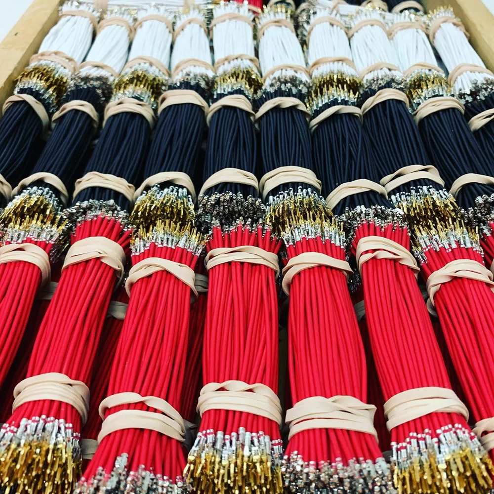
Managing kitting and packaging in-house can be time-consuming, costly, and error-prone.
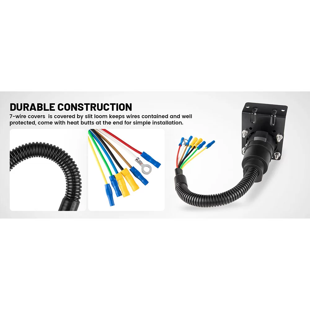
Maybe an off-the-shelf cable can't meet your needs.
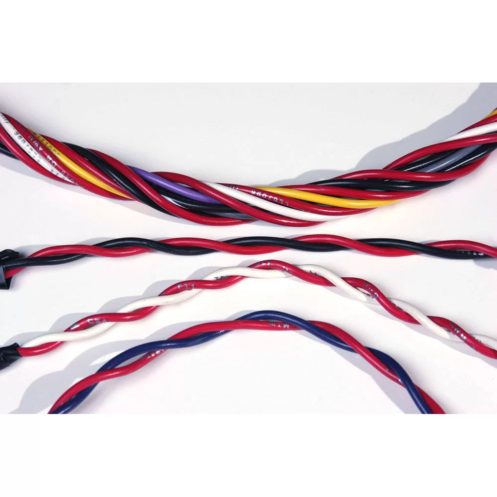
Twisting entwines multiple wires and arranges them tightly next to each other. Depending on the AWG size, we can group up to fifty conductors.
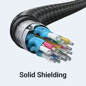
Shielding refers to the metallic layer surrounding a cable’s conductor, created to limit signal interference between the wire and external fields.
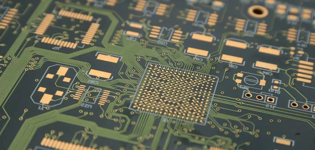
PCB manufacturing is the process of building a physical PCB from a PCB design according to a certain set of specifications.

The following design standards refer to the IPC-SM-782A standard and the design of some famous Japanese design manufacturers and some better design solutions accumulated in the manufacturing experience.
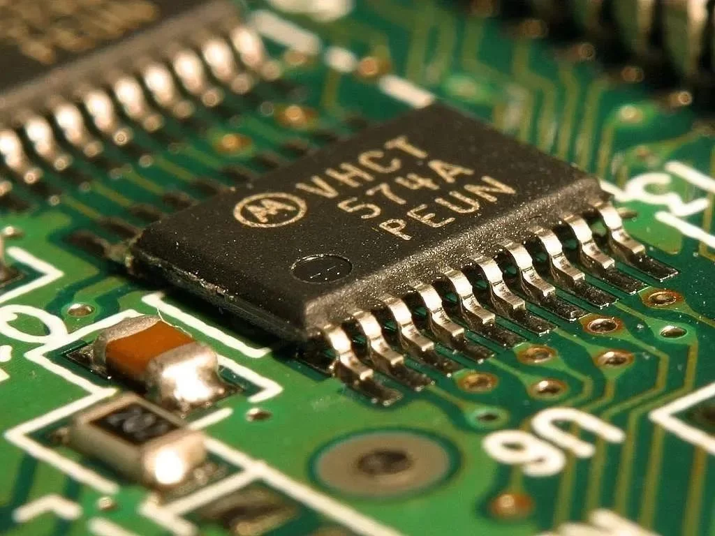
Via holes, also known as through holes, play a role in connecting different parts of a circuit board.

