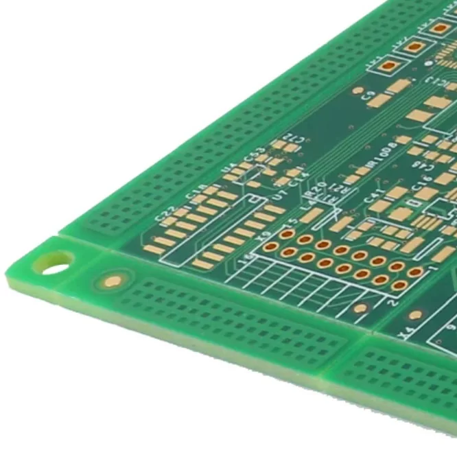
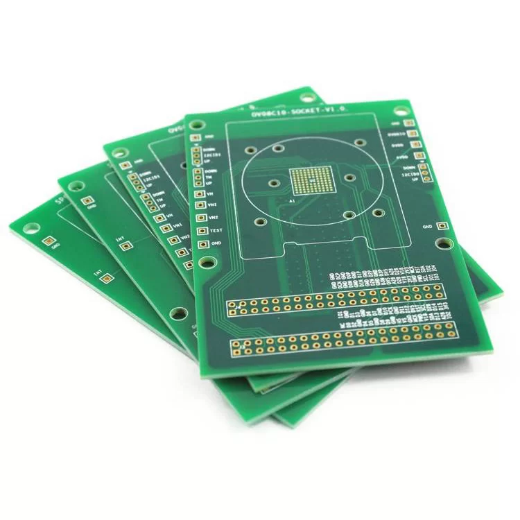
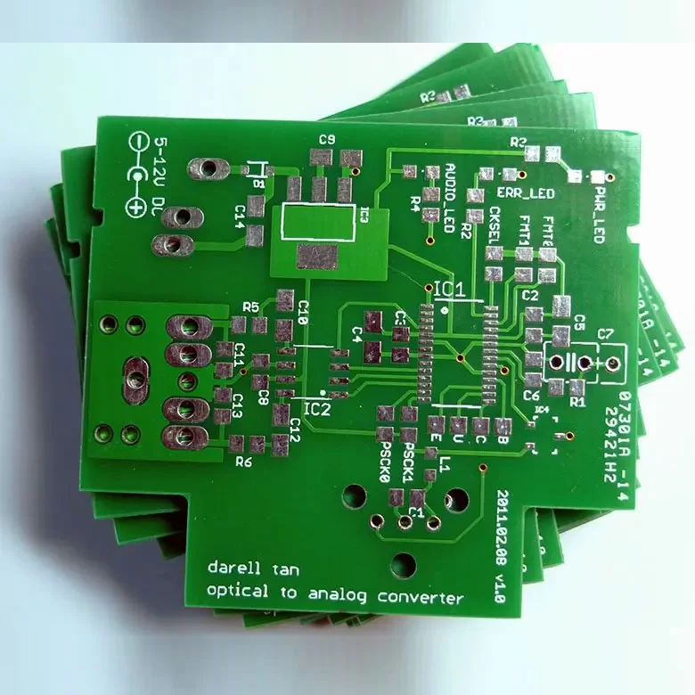
94V0 FR4 PCB
Datasheet
Model: FR-4 PCB
Layers: 1–32 layers
Material:Shengyi,Tuc,ITEQ,Panasonic
Finished Thickness:0.4-3.2mm
Copper Thickness: 0.5–6.0 oz (inner layer: 0.5–2.0 oz)
Color: Green/White/Black/Red/Blue
Surface treatment: LF-HASL/ENIG/OSP/ENEPIG/Immersion Tin
What's FR-4 PCB?
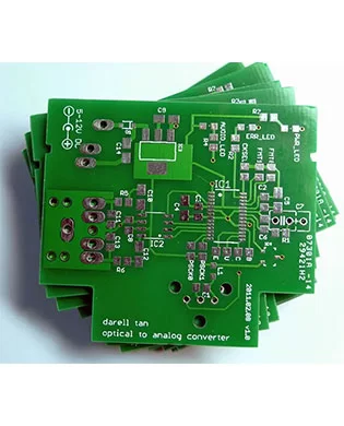
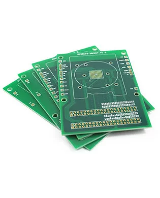
FR-4 stands out as one of the most versatile options. The composition of an FR-4 printed circuit board comprises a woven glass fabric reinforcement impregnated with a flame-retardant epoxy resin binder.It has excellent mechanical strength, heat resistance, corrosion resistance, and electrical performance, making it widely used in electronic products.
Features
1. Safety and Stability
Crafted from flame-retardant epoxy resin, it delivers excellent fire and heat resistance; meanwhile, it tolerates high temperatures during soldering and long-term operation, effectively warding off delamination, solder joint failure and fire hazards, thus ensuring the safe and stable operation of electronic devices.
2. Structural Reliability
Boasting high mechanical strength and durability, it resists vibration and impact to avoid damage during handling, assembly and operation. Its low Coefficient of Thermal Expansion (CTE) also endows it with dimensional stability across a wide temperature range, ensuring precise alignment of circuit features
3. Excellent Electrical Performance
With high electrical insulation resistance and a low dielectric constant, it ensures reliable insulation between conductive traces and minimizes signal interference, providing solid support for the stable operation of electrical circuits, especially high-frequency and precision circuits.
4. Practicality and Adaptability
It simplifies manufacturing processes like drilling, etching and routing, reducing production costs and labor; globally wide availability enhances its cost-effectiveness. Moreover, it is compatible with lead-free soldering (compliant with RoHS) and can be made into single-sided, double-sided or multilayer configurations to adapt to diverse needs.
Application
1. Communications Industry:Routers, network switches, 5G base station signal processing modules, optical fiber communication transceivers.
- 2. Automotive Industry:In-vehicle navigation systems, engine control systems, Electronic Stability Program (ESP), in-vehicle entertainment hosts.
- 3. Aerospace & Defense Industry:Aircraft avionics systems, satellite communication terminals, radar signal processing boards, military portable communication devices.
- 4. Industrial Manufacturing Industry:Automated production line control modules, motor drivers, industrial robot sensor interface boards, intelligent flow meters.
- 5. Energy Industry:Solar inverters, wind power control cabinets, power grid load monitoring equipment, energy storage battery management modules.
- 6. Security & Protection Industry:HD surveillance cameras, face recognition access control machines, infrared alarm controllers, intelligent inspection robot main control boards.
- 7. Consumer Electronics Industry:Smartphone motherboards, laptop keyboard control boards, smart TV signal decoding boards, smart home devices.
- 8. Medical Industry:Patient ECG monitors, blood analyzers, ultrasonic diagnostic instrument probe control boards, infusion pump intelligent control modules.
Challenge
1. Limited High-Frequency Performance
With a relatively high dielectric constant, signal attenuation and impedance fluctuation easily occur at frequencies above several gigahertz (GHz), restricting high-speed signal transmission and bandwidth of RF/microwave circuits.
- 2. Moisture Absorption IssueProne to absorbing atmospheric moisture, leading to changed electrical properties. In harsh environments or thermal cycling, it further causes delamination, solder joint failure and increased dielectric loss, reducing stability and lifespan.
- 3. Poor Thermal ConductivityLower thermal conductivity than specialized substrates (e.g., metal-core PCBs) results in localized "hotspots" during operation. This accelerates component aging and may cause failures in high-power/high-density designs.
- 4. Environmental, Mechanical & Processing ConstraintsEnvironmental: Epoxy resins release VOCs during production (polluting if untreated); composite structure complicates disposal/recycling.Mechanical: Inherently brittle (worse in thin/high-glass-content laminates), prone to cracking/warping under stress/impact.Processing: Requires strict temperature/humidity control and specialized equipment for precise drilling/etching, increasing fabrication cost and complexity.
Process of FR-4 PCBs
1. Material Selection
Select base materials and copper foils dictates the mechanical strength, electrical conductivity, and thermal stability of the circuit board.
2. Inner Layer Fabrication
Multilayer PCB manufacturing begins with inner layer fabrication. The designed circuit layout is initially patterned onto the inner copper foil layers. Through photoplotting and exposure processes, the circuit design is accurately transferred to the copper foil on the base material.
3. Inner Layer Etching
Unwanted copper foil is removed through a chemical etching process, retaining only the desired circuit traces. This is a critical step in PCB manufacturing, as any deviation can result in circuit open circuits or short circuits.
4. Lamination
Lamination is a critical step in multilayer PCB production. Individual inner layers are stacked together with prepreg sheets and bonded into an integrated structure using a high-temperature, high-pressure laminating machine. During lamination, strict attention must be paid to ensuring precise alignment between circuits of different layers.
5. Drilling
Drilling serves to create through-holes in the PCB, facilitating the connection of circuits across different layers or the mounting of electronic components. High-precision CNC drilling machines can drill the required holes quickly and with high precision.
6. Plating
After drilling, a conductive material (typically copper) is deposited onto the inner walls of the holes via electroplating, establishing electrical continuity through the holes. This step ensures reliable current transmission between the layers of the PCB.
7. Outer Layer Circuit Fabrication
Analogous to inner layer fabrication, the outer circuit pattern is precisely transferred to the copper foil surface of the PCB through photoplotting and exposure techniques. The outer circuit is then etched using a chemical etching process identical to that used for the inner layers.
8. Solder Mask
Solder mask is applied to protect copper conductors from oxidation and prevent unintended short circuits during the soldering process.
9. Silkscreen
Silkscreen marking involves printing component identifiers, pin numbers, and other essential information onto the PCB. This is crucial for post-manufacturing assembly and maintenance work.
10. Surface Finish
To enhance soldering performance and prevent copper oxidation, common PCB surface finish techniques include tin plating, gold plating, and immersion silver.
11. Testing
This step primarily verifies the electrical continuity of each circuit path, ensuring the absence of short circuits or open circuits.
If you have any camping barbeque equipment inquiry, please feel free to contact us.
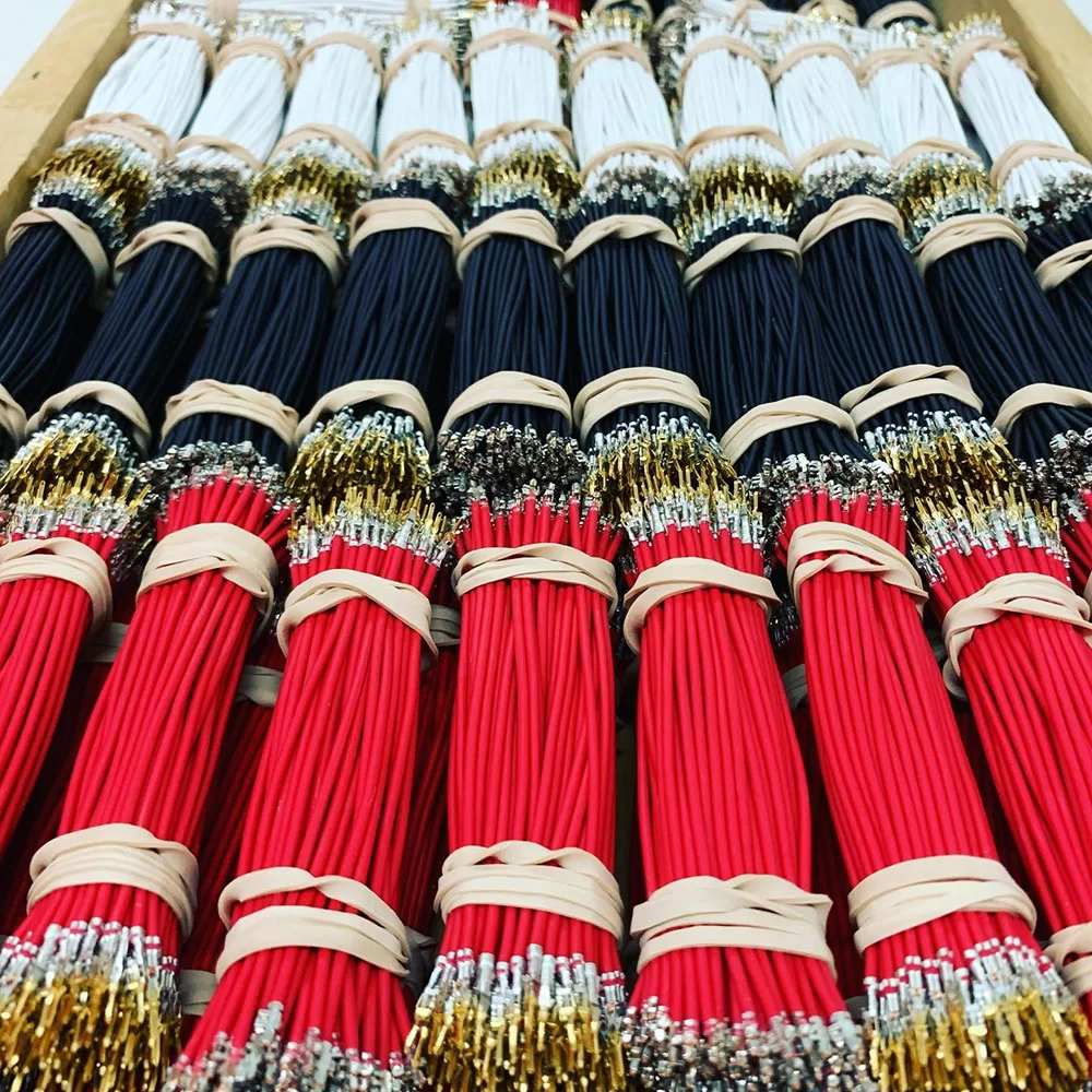
Managing kitting and packaging in-house can be time-consuming, costly, and error-prone.
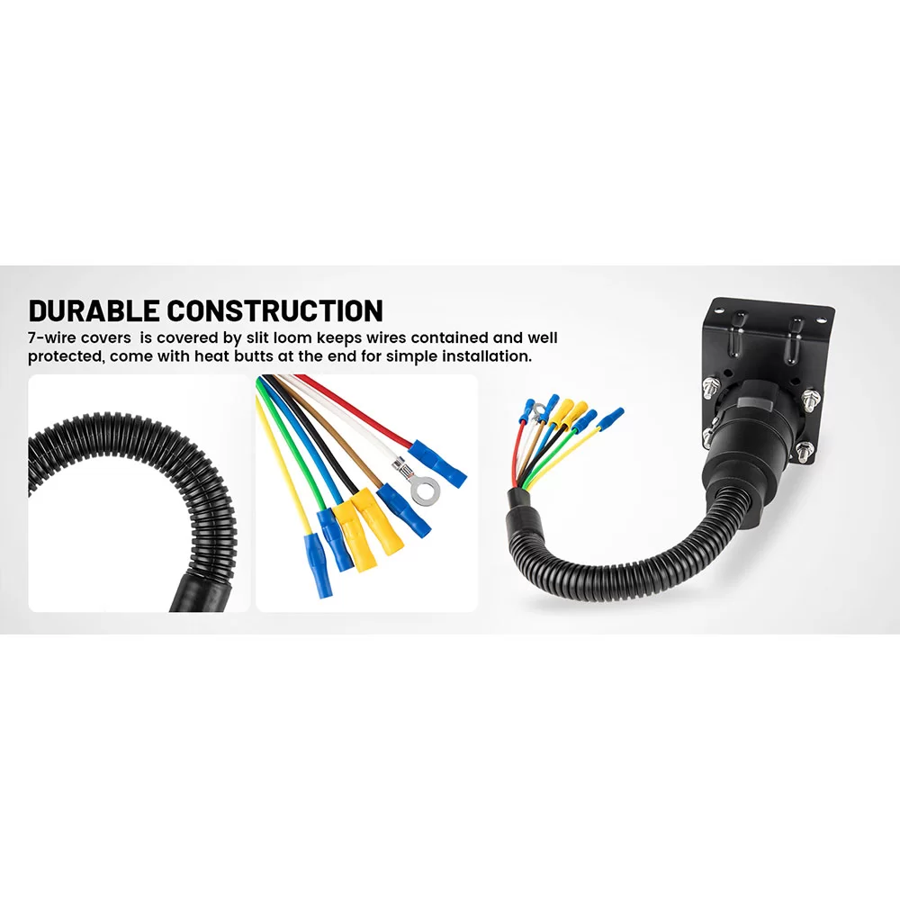
Maybe an off-the-shelf cable can't meet your needs.
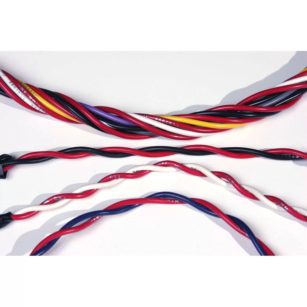
Twisting entwines multiple wires and arranges them tightly next to each other. Depending on the AWG size, we can group up to fifty conductors.
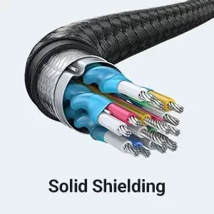
Shielding refers to the metallic layer surrounding a cable’s conductor, created to limit signal interference between the wire and external fields.
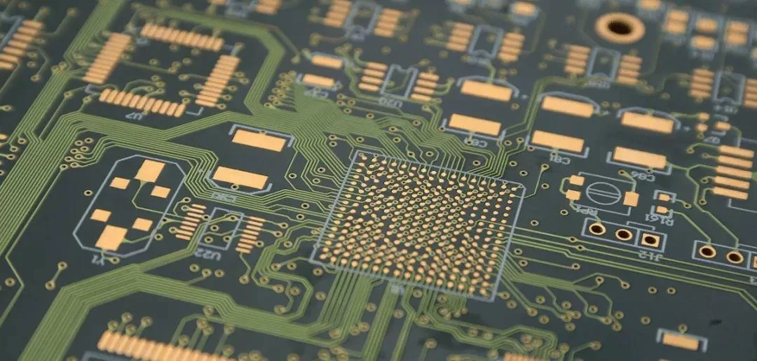
PCB manufacturing is the process of building a physical PCB from a PCB design according to a certain set of specifications.

The following design standards refer to the IPC-SM-782A standard and the design of some famous Japanese design manufacturers and some better design solutions accumulated in the manufacturing experience.
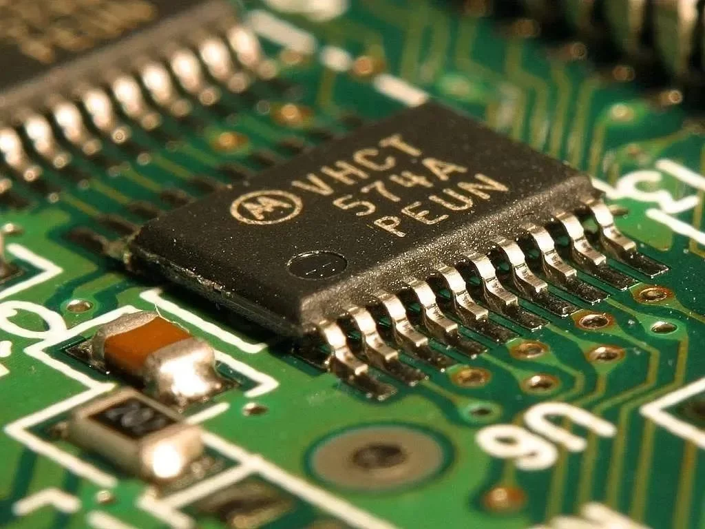
Via holes, also known as through holes, play a role in connecting different parts of a circuit board.

