IC Substrate PCB
What's IC substrate PCB
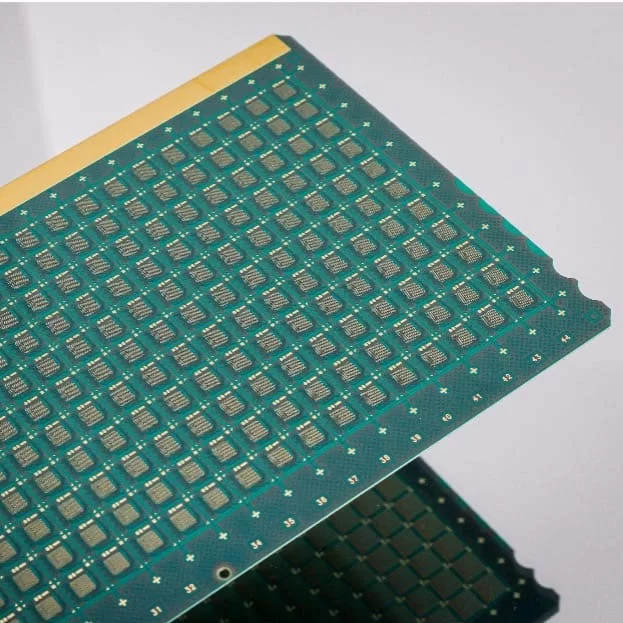
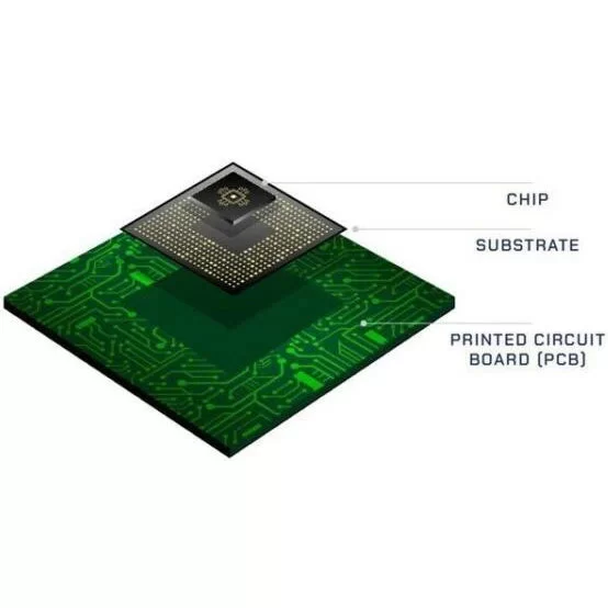
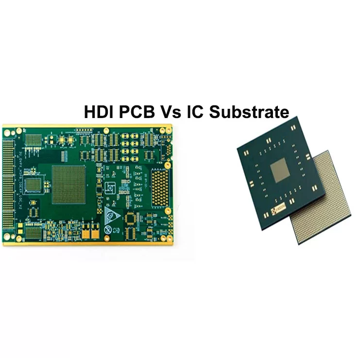
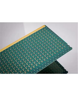
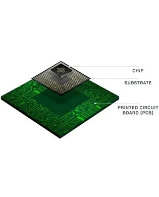
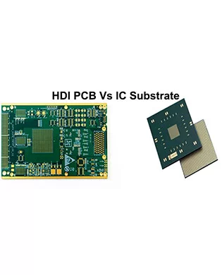
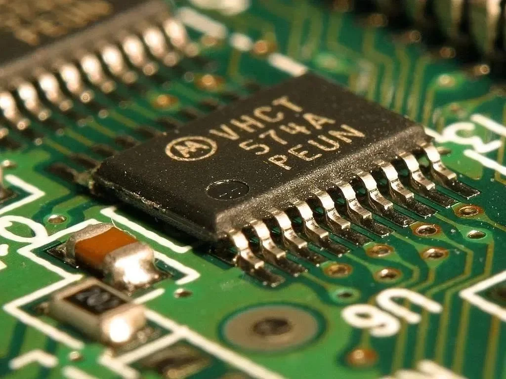
IC substrate PCB is simply the base material of the IC package, providing connections between the PCB and the IC package on the printed circuit board. For example, it resembles a high-density circuit board with surface-mount components. Integrated circuits such as ball grid arrays and chip-scale packages benefit from this.
The IC substrate's fabrication determines the IC's performance, and it is denser than typical high-density PCBs.
Advantages
1.Miniaturization for Compact
2.Excellent Thermal Management
3.Superior Electrical Performance
4.High Reliability
Application
IC substrates (PCBs) are widely used in many fields, such as smartphones, tablets, networking equipment, small telecommunications equipment, medical equipment, aerospace, aviation, and military equipment. System-level applications include processor BAs, memory devices, graphics cards, gaming chips, and external sockets.
Process
IC substrate PCB takes extra care because these boards are much thinner and more precise than regular PCBs. Let’s walk through the basic steps.
Core Material Lamination: It all starts with stacking very thin layers of copper and resin. These are pressed together using heat to form a solid base. Since the material is so thin, even small mistakes can cause bending or warping.
- Via Drilling: Tiny holes called vias are drilled to connect the layers. Laser drilling is used for very small holes, while mechanical drilling works for the bigger ones. These help create the complex pathways inside the board.
- Copper Plating and Etching: Once the holes are drilled, they’re coated with copper to make them conductive. Then, the board is etched to remove extra copper and form the actual circuits that will carry signals.
- Solder Mask Application: A solder mask is added to protect the board and keep solder from going to the wrong places. The height difference between the pad and the mask must be super small—this helps ensure clean connections.
- Surface Finishes (ENIG, ENEPIG): To protect the exposed copper and make soldering easier, surface finishes like ENIG or ENEPIG are applied. These finishes also help prevent oxidation.
- Final Inspection and Testing: The last step is testing. Each board is carefully checked to make sure it works properly, looks right, and meets all the size and thickness rules.
Future Trends in IC Substrate PCB Technology
Powering New Technologies
IC substrate PCBs are a great fit for AI hardware, AR/VR devices, and even quantum computers. These technologies need speed, small size, and stable signals—all things these boards can handle well.
Growth of Substrate-Like PCBs (SLPs)
A newer option called SLPs (Substrate-Like PCBs) is gaining attention. They offer many of the same benefits as IC substrate PCBs but at a lower cost. SLPs are likely to become more common in future tech products.
Focus on Eco-Friendly Solutions
More companies are looking for green materials and ways to recycle PCBs. The goal is to reduce waste and make production better for the environment without losing performance.
If you have any camping barbeque equipment inquiry, please feel free to contact us.
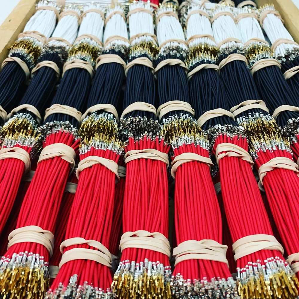
Managing kitting and packaging in-house can be time-consuming, costly, and error-prone.
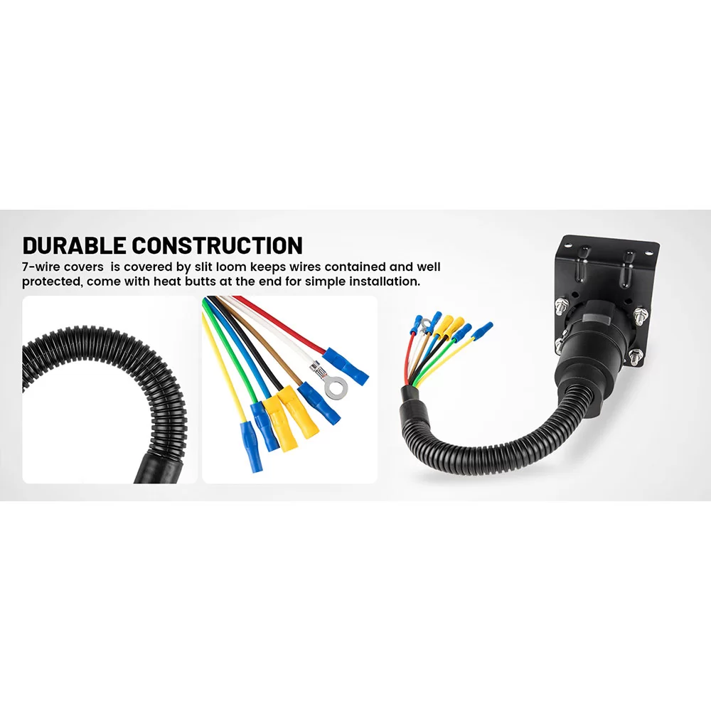
Maybe an off-the-shelf cable can't meet your needs.
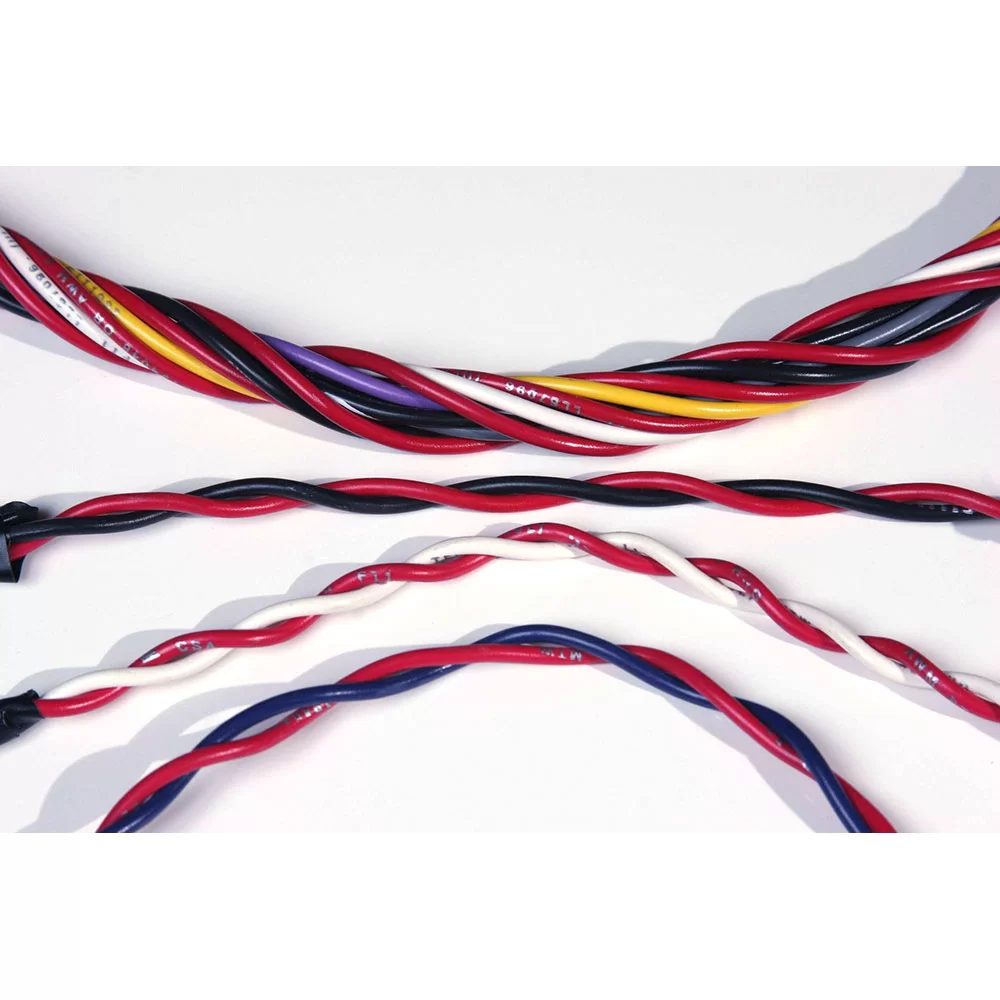
Twisting entwines multiple wires and arranges them tightly next to each other. Depending on the AWG size, we can group up to fifty conductors.
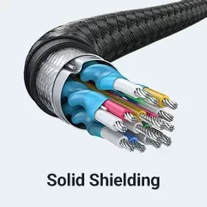
Shielding refers to the metallic layer surrounding a cable’s conductor, created to limit signal interference between the wire and external fields.
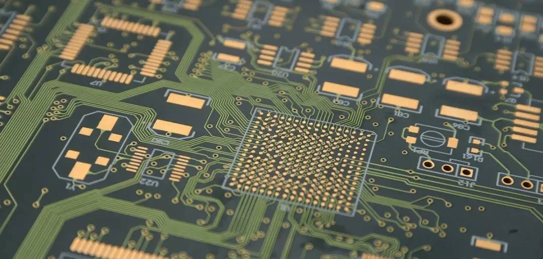
PCB manufacturing is the process of building a physical PCB from a PCB design according to a certain set of specifications.

The following design standards refer to the IPC-SM-782A standard and the design of some famous Japanese design manufacturers and some better design solutions accumulated in the manufacturing experience.
Via holes, also known as through holes, play a role in connecting different parts of a circuit board.

