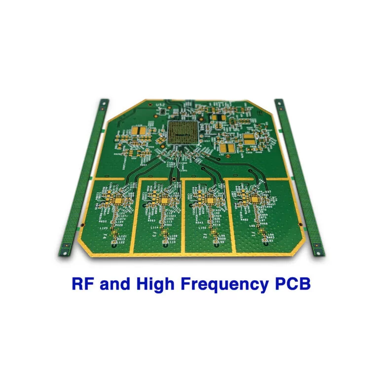
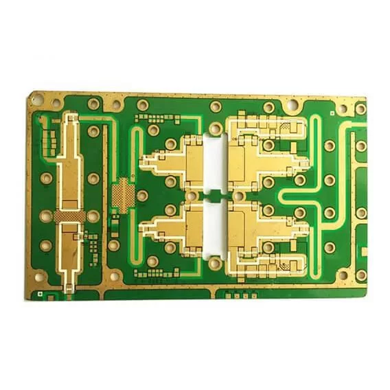
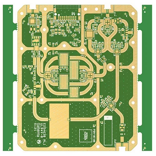
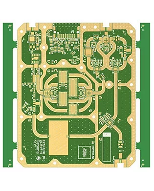
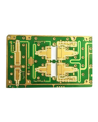
High Frequency FR4 PCB
Data Sheet
Model: high frequency PCB
Material: high frequency PCB materials
Quality standard: IPC 6012 Class2
- high frequency pcb dk: 2.0 -1.6
- Layers:1 Layer pcb-36 layer pcb
- Thickness:0.254mm-12mm
- Copper thickness: base copper 0.5oz/ 1oz
- Surface technology: Silver, Gold,OSP
- Special process: mixed material, stepped groove
- Application: High Frequency PCB,microstrip antenna
Why do we need High-Frequency PCBs?
Electronic circuits behave very differently at high frequencies. This is mainly due to a change in the behavior of the passive components (resistors, inductors, and capacitors).
It also has parasitic effects on the following:
Active components
PCB tracks
Grounding patterns
Signals are vulnerable to noise and come with much tighter impedance tolerance as compared to conventional circuit boards. Signals between two objects would always get disrupted due to the noise caused by high frequency. This takes more energy, so a higher-frequency wave has more energy than a lower-frequency wave with the same amplitude.
Material Selection for High-Frequency PCB’s
For the production of High-frequency PCB boards, there are special materials required which give high-speed signals. Some of the materials are as follows:
Rogers 4350B HF: Similar to the FR4, this material also has a low fabrication cost. It also offers excellent dimensional stability.
- Taconic TLX: This material consists of PTFE fiberglass, it is physically a stable material providing the best thermal, mechanical, and electrical properties. However, the only problem it has is, being difficult to fabricate.
- Taconic RF-35 Ceramic: This is a low-cost material that is made of ceramic-filled PTFE and glass. It is easy to fabricate but it has moderate peel strength, perfect electrical performance as well as low power dissipation.
- Rogers RO3001: This consists of a bonding film with a comparatively low dielectric constant. It is also highly resistant to chemicals and high temperatures.
- ARLON 85N: The ARLON 85N has a very high thermal resistance. It is made of pure polyamide resin.
Characteristics of different high-frequency PCB materials
1. High-Frequency FR-4 PCB
Features: Based on standard FR-4, this material utilizes a modified resin with a dielectric constant (Dk) of 3.8-4.5, a dissipation factor (Df) of 0.015-0.025, and excellent temperature resistance (Tg ≥ 170°C). Its cost is only 20%-30% higher than standard FR-4.
Applications: High-frequency devices in mid- and low-band frequencies, such as WiFi 6 routers and 4G base station peripheral modules.
2. Polytetrafluoroethylene (PTFE) PCB
Features: Extremely low Dk (2.0-2.3), extremely low Df (0.001-0.003), and virtually minimal signal loss. Temperature resistance ranges from -260°C to 260°C. However, processing is difficult and the cost is high (3-5 times that of high-frequency FR-4).
Applications: Ultra-high frequency/precision applications, such as 5G millimeter-wave base stations, satellite communications, and radar equipment.
- 3. Hydrocarbon Resin PCBFeatures: Dk 3.0-3.5, Df 0.003-0.008, performance between PTFE and high-frequency FR-4, good processability (drillable like ordinary FR-4), and 40% lower cost than PTFE.Applications: 5G macro base stations, optical modules, and high-end routers.
- 4. Polyphenylene Oxide (PPE/PPO) PCBFeatures: Dk 2.4-3.0, Df 0.005-0.01, excellent moisture resistance, 20% lower cost than hydrocarbon resin, but slightly lower temperature resistance (Tg 120-150°C).Applications: High-frequency modules for consumer electronics, such as 5G RF components in smartphones and drone image transmission modules.
- 5. Ceramic-filled PCBFeatures: Stable Dk (adjustable from 2.5 to 6.0) and a low temperature coefficient (≤50ppm/°C), suitable for applications requiring precise impedance control. However, this material can be brittle and heavy.Applications: Automotive radar (77GHz), Industrial IoT gateways.
Application
High frequency PCBs are always used in the following applications
Automotive Radar Systems
Global Positioning Satellite Antennas
- Cellular Telecommunications Systems – Power Amplifiers and Antennas
- Direct Broadcast Satellites
- E-band Point to Point Microwave Links
- RF Identification (RFID) Tags
- Airborne and Ground Based Radar Systems
- Millimeter Wave Applications
- Missile Guidance Systems
- Space Satellite Transceivers
The main material of high-frequency PCB board is high-frequency copper clad laminate, and its core requirements are to have low dielectric constant (DK) and low dielectric loss factor (DF). In addition to ensuring lower Dk and Df, the consistency of Dk parameters is also one of the important factors to measure the quality of the PCB board. In addition, another important parameter is the impedance characteristics of the PCB board and some other physical characteristics.
Benefits of using
The reason high-frequency PCBs are used widely in the world of science, and Electronics in general, is owing to the tons of advantages we see in them. Some of them include
Moderately low in cost; therefore, can be mass-produced
- Reusable; hence can be utilized multiple times
- Highly durable and thus giving a great shelf life of the circuit.
- Compact size decreases the wastage of wire.
- The above well-grounded factors are the reason that brings certainty in the execution of the electronic/electric circuit.
If you have any camping barbeque equipment inquiry, please feel free to contact us.
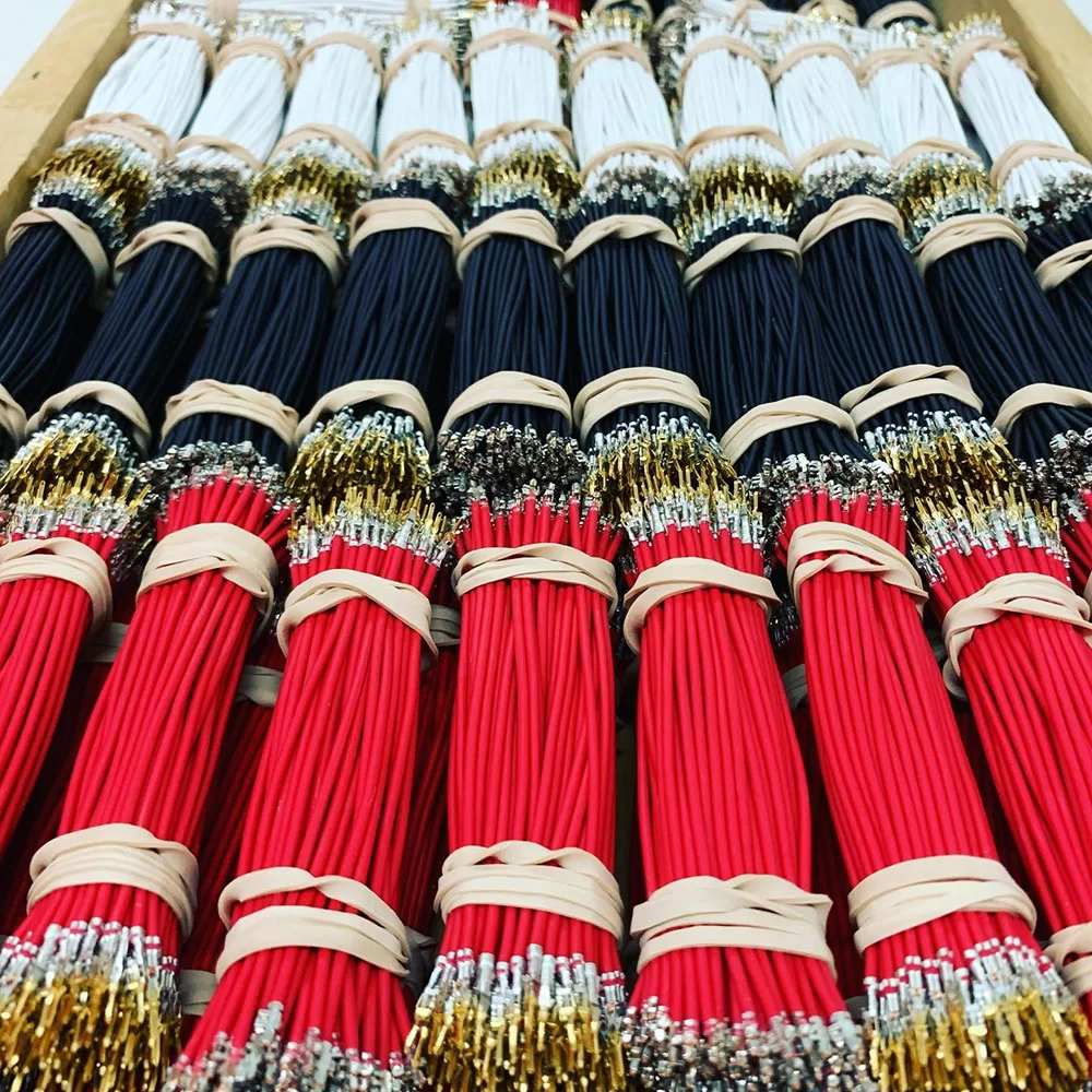
Managing kitting and packaging in-house can be time-consuming, costly, and error-prone.
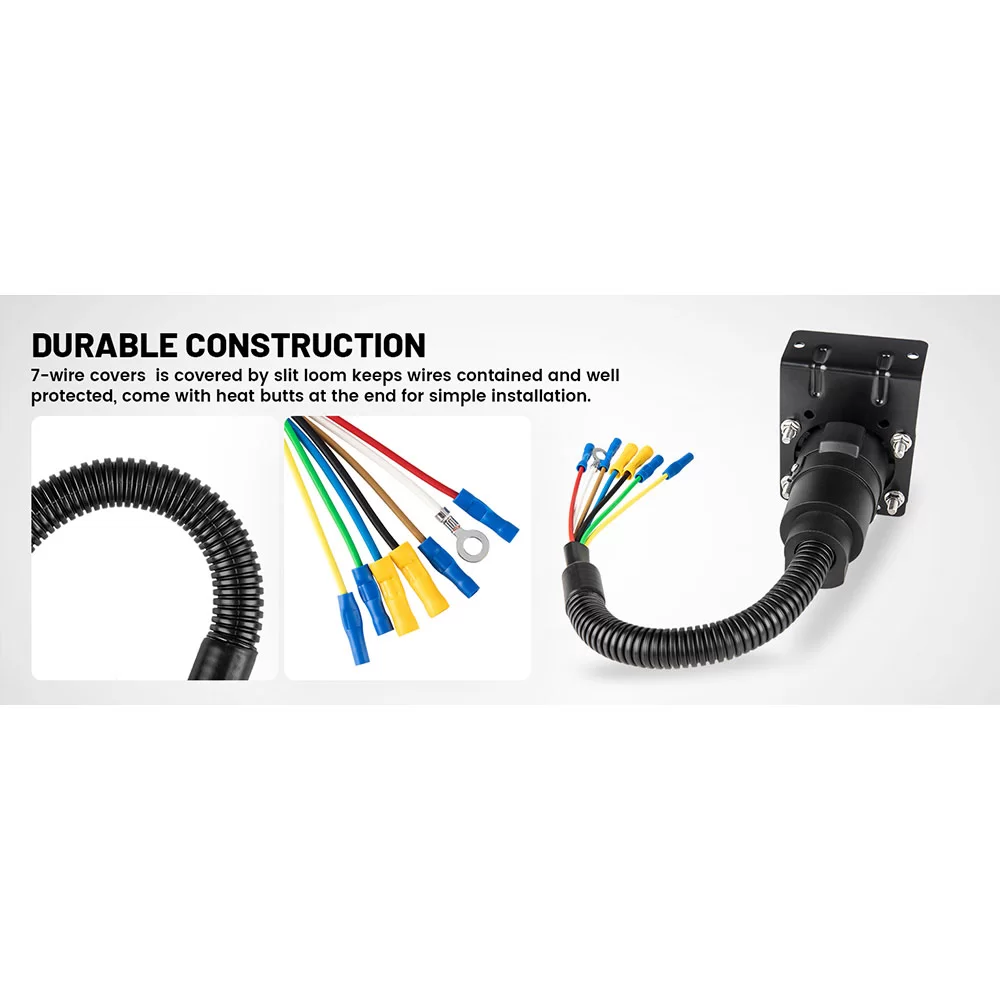
Maybe an off-the-shelf cable can't meet your needs.
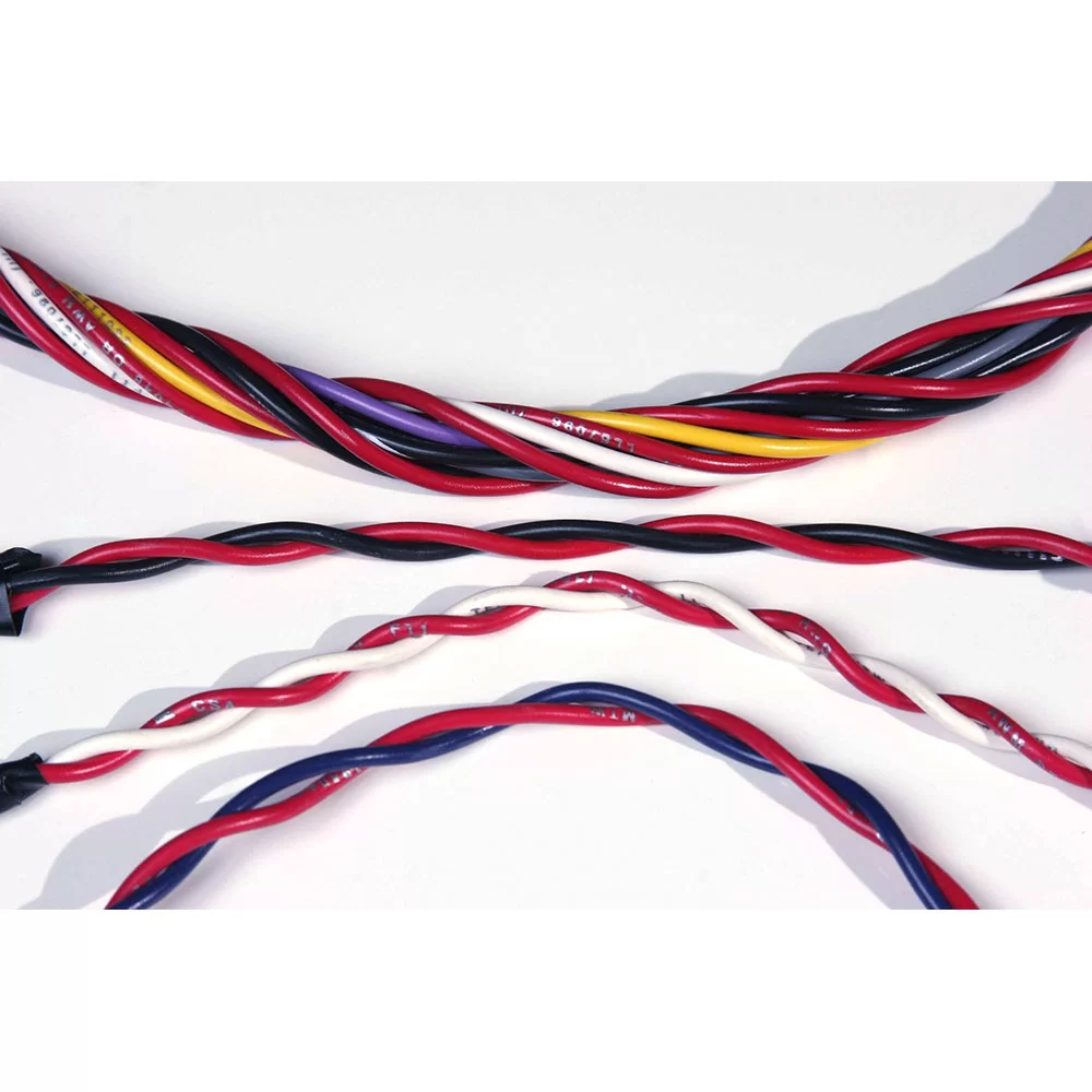
Twisting entwines multiple wires and arranges them tightly next to each other. Depending on the AWG size, we can group up to fifty conductors.
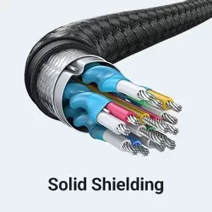
Shielding refers to the metallic layer surrounding a cable’s conductor, created to limit signal interference between the wire and external fields.
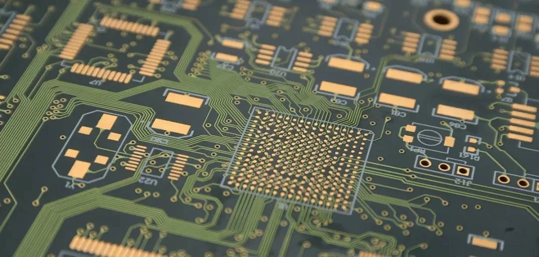
PCB manufacturing is the process of building a physical PCB from a PCB design according to a certain set of specifications.

The following design standards refer to the IPC-SM-782A standard and the design of some famous Japanese design manufacturers and some better design solutions accumulated in the manufacturing experience.
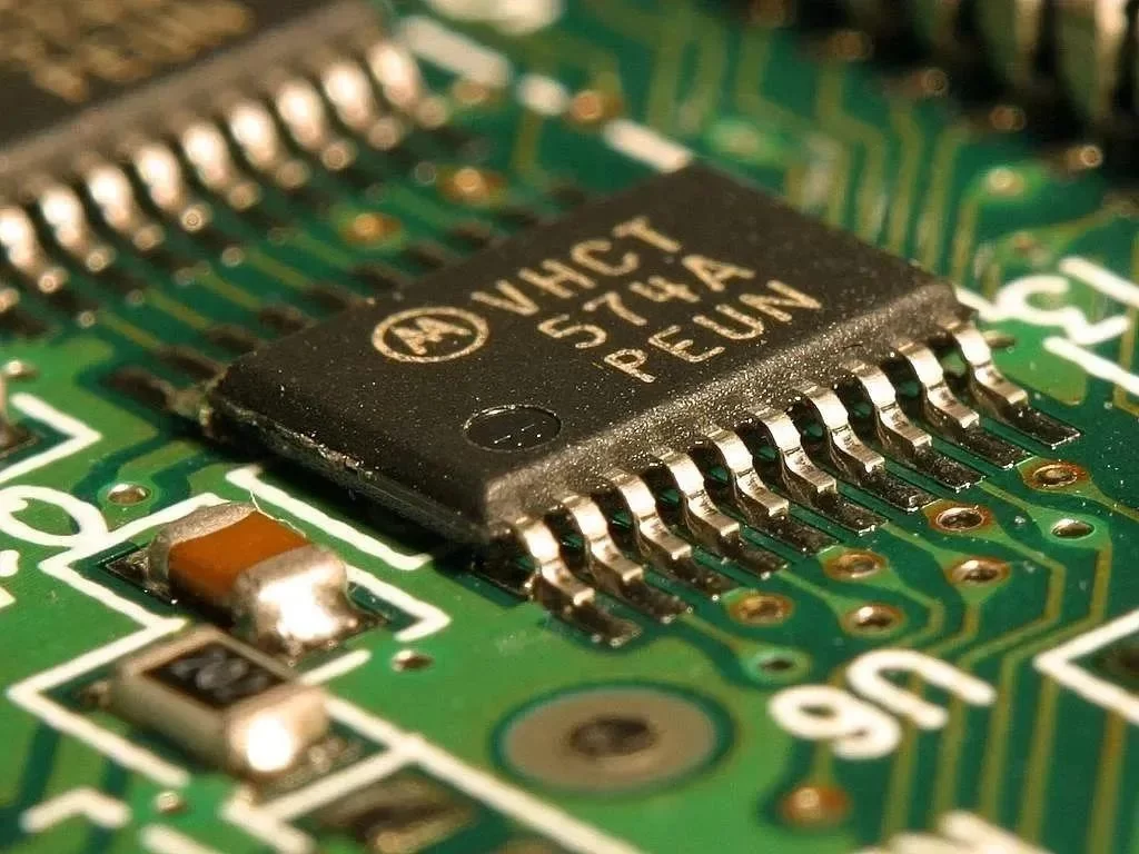
Via holes, also known as through holes, play a role in connecting different parts of a circuit board.

