Flex PCBA
What is Flexible PCB Assembly?
Flexible PCB assembly refers to the assembly of flexible printed circuit boards. It uses a flexible substrate as the base material to structurally support electronic components and achieve electrical connections between them. The flexible substrate is typically a polyimide (PI) film laminated with a copper film and patterned through an etching process. Flexible PCBs appear as a thin, translucent, amber-colored material that is easily bent.
What are the advantages of flexible PCB assembly?
1.Flexibility
The term "flexible PCB" stems from its primary advantage: flexibility. Flexible PCBs can be easily twisted and bent, something rigid PCBs cannot do. This flexibility benefits space-saving systems where flexible PCBs can easily conform to the contours and geometry of a surface.
2.Lightweight
Flexible PCBs are lighter than rigid PCBs. They are suitable for portable and easy-to-install devices. Their light weight and thin profile contribute to a sleek and aesthetically pleasing appearance.
3.Resistance to Harsh Environments
Polyimide is used to protect copper conductors from harsh conditions. It is a material that can withstand high temperatures and resist chemical corrosion. Flexible circuit assemblies are suitable for aerospace and extreme temperature applications.
- 4.Small Overall SizeFlexible PCBs are flexible and thin, resulting in a smaller overall size. They can be easily shaped to fit thin screens such as laptops and tablets, as well as compact wearable devices.
What are the assembly processes for flexible PCBs?
The assembly process for flexible PCBs is basically the same as that for rigid PCBs, from solder paste printing to component pick and place, reflow soldering, AOI inspection, and final testing. However, during production, it is crucial to maintain the flatness of the flexible PCB, as even slight unevenness can lead to serious defects.
Solder Paste Printing
Polyimide, the polymer material that makes up flexible PCBs, is a "hygroscopic" material, meaning it easily absorbs moisture. The flexible PCB must first be baked to dry the moisture on the polyimide substrate, typically at around 120 degrees Celsius. Solder paste is then printed onto the flexible substrate using a stainless steel stencil and rubber squeegee. In each SMT process, the flexible PCB must be carefully held in place using special fixtures.
Pick-and-Place
Using a component placement machine, electronic components are picked up and placed into the flexible PCB with wet solder paste. The machine integrates intelligent vision systems and software to accurately position components. An efficient pick and place process often determines the overall throughput of an SMT production line, so optimizing procedures to speed up the process is crucial.
Solder Reflow
Wet solder paste must melt and solidify to achieve a reliable connection. The solder paste's technical datasheet indicates the recommended curing profile, along with the specified duration and temperature. It's best to perform prototype simulations to understand the solder paste and component behavior and determine the temperature distribution during the actual reflow process. An initial preheating phase is required to vaporize the solder paste's flexible material. The temperature then peaks to completely melt the solder paste, followed by cooling until it fully solidifies.
Automated Optical Inspection
Automated Optical Inspection (AOI) machines should be used to inspect mounted circuit boards to verify that parts are correctly placed and oriented. AOI can also detect solder bridging, missing components, and foreign objects. AOI challenges during flexible circuit assembly include uneven lighting due to the reflective surface of polyimide substrates.
PCBA Testing
Flexible printed circuit assembly processes can introduce defects on flexible PCBs that are not detectable through visual inspection alone. The assembled circuit board must undergo electrical testing to check for any circuit problems that may affect product quality.
If you have any camping barbeque equipment inquiry, please feel free to contact us.
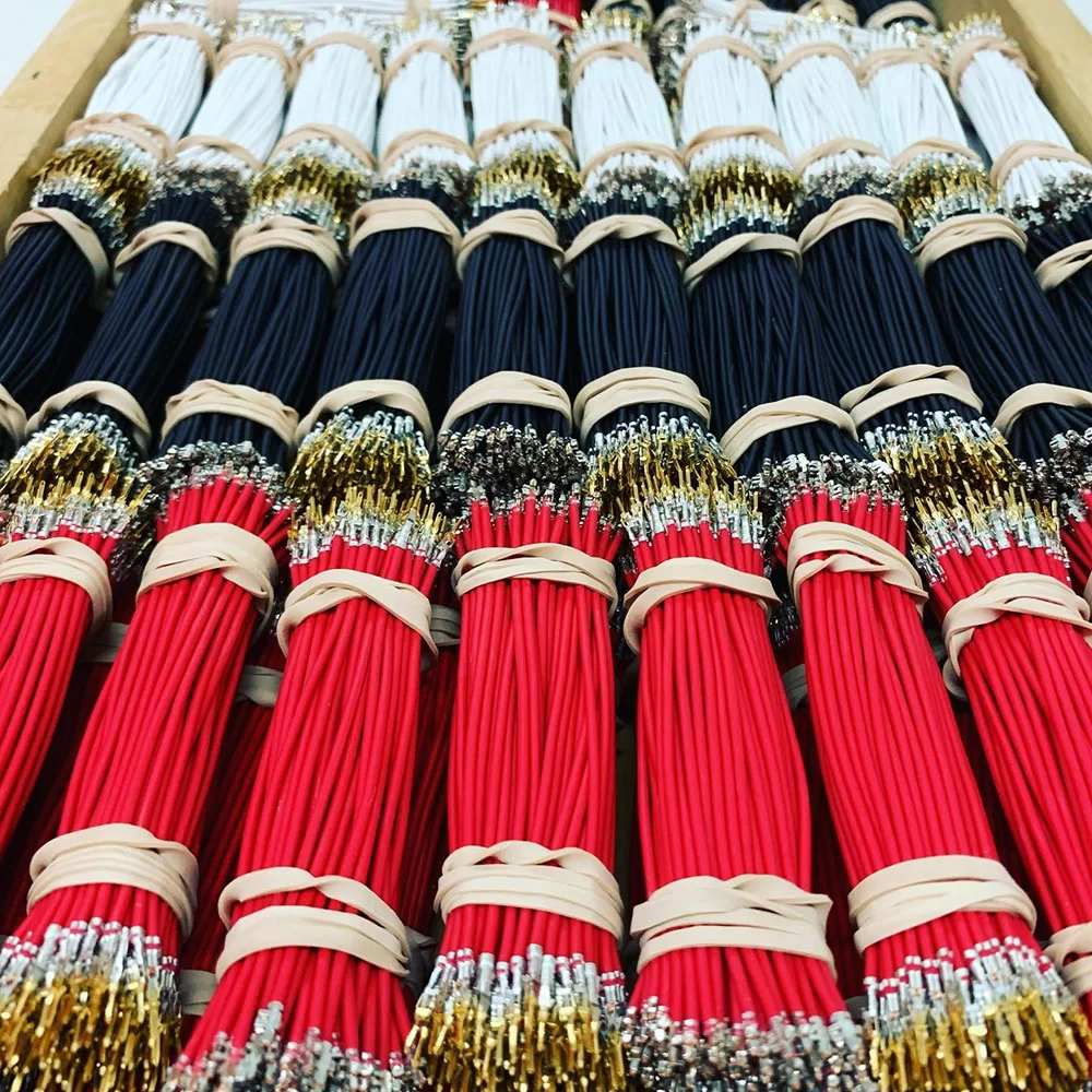
Managing kitting and packaging in-house can be time-consuming, costly, and error-prone.
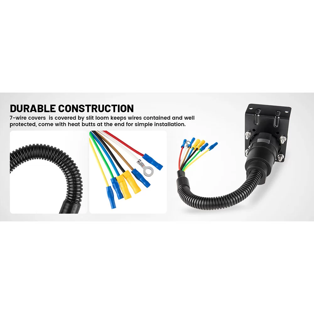
Maybe an off-the-shelf cable can't meet your needs.
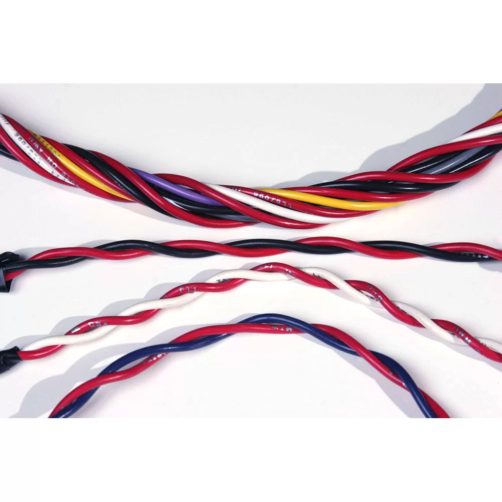
Twisting entwines multiple wires and arranges them tightly next to each other. Depending on the AWG size, we can group up to fifty conductors.
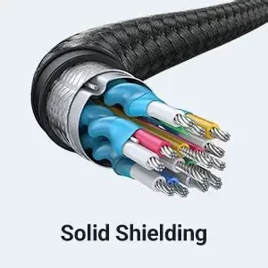
Shielding refers to the metallic layer surrounding a cable’s conductor, created to limit signal interference between the wire and external fields.
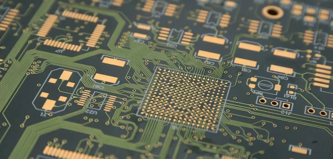
PCB manufacturing is the process of building a physical PCB from a PCB design according to a certain set of specifications.

The following design standards refer to the IPC-SM-782A standard and the design of some famous Japanese design manufacturers and some better design solutions accumulated in the manufacturing experience.
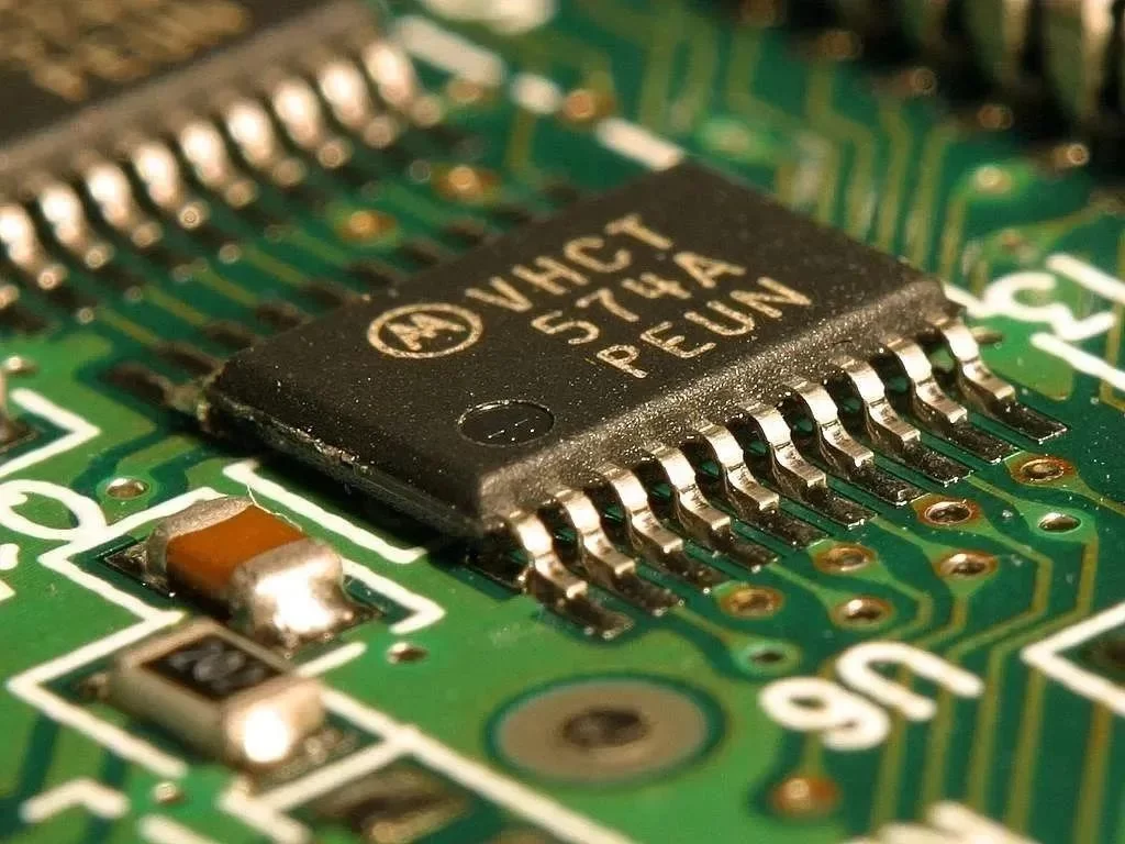
Via holes, also known as through holes, play a role in connecting different parts of a circuit board.


