which has lower cost of electricity, water and labor.
And factory are self-built, no house rent.
--- Export Rebates: Our company is value-added tax general taxpayer, so we can handle export rebates due to national policy support.
managers & hundreds of long term cooperation customer.
I believe we can do long term business!
But you can use these files to request a quotation. If you do not have gerber file, you can send us sample to copy it.
But you can use these files to request a quotation. If you do not have gerber file, you can send us sample to copy it.
PCBA sample photos if possible. By allowing us to see the product pictures it will help us to give you the quotation faster.
In addition to the above, we would need details of approximate order quantity.
This is quite common for prototype orders. Please keep an eye on your email in the first 12 hours after placing your order.
The shape should be clearly indicated in at least one of your copper layers. Otherwise you must supply a mechanical plan, separate from the Gerber file, indicating the shape of the PCB.
This file has to have a reference to the copper layers, or has to have the same offset as the other layers.
For multi-layer boards please ensure you have adequate back set for the bevels. Please mention this in the order form when placing your order.
PCBA(printed circuit board assembly): PCB information, BOM, (Testing documents...)
2. BOM list. (Excel(PDF, WORD, TXT)
3. Clear pictures of PCBA or PCBA samples to us.
4. Pick N Place file.
5. Test procedure for PCBA.
(1)Sample
1-2 Layers: 5 to 7working days
4-8 Layers: 10 working days
(2)Mass production: 15~30days depens on QTY
PCB Manufacturing Service PCB layout, PCB design according to your idea
PCB copy/clone Digital Circuit Design, System Hardware Design...
PCB Assembly Service Electronic, components material purchasing, Bare PCB fabrication, PCB Assembly Service. (SMT, BGA, DIP)
FULL Test: AOI, In-Circuit Test (ICT), Functioal Test (FCT)
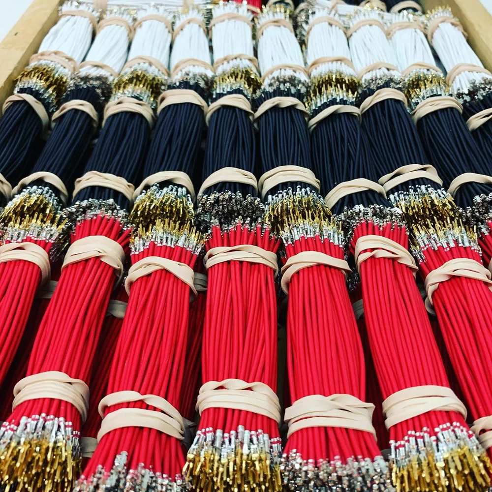
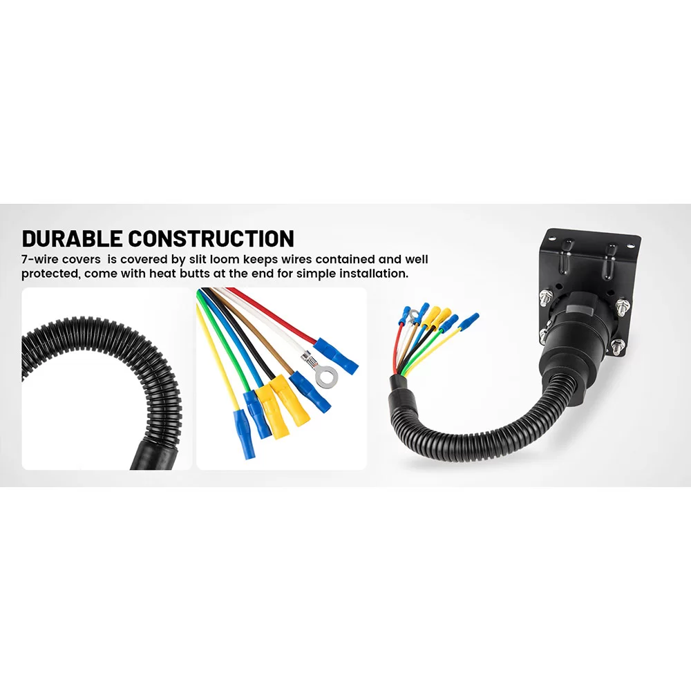
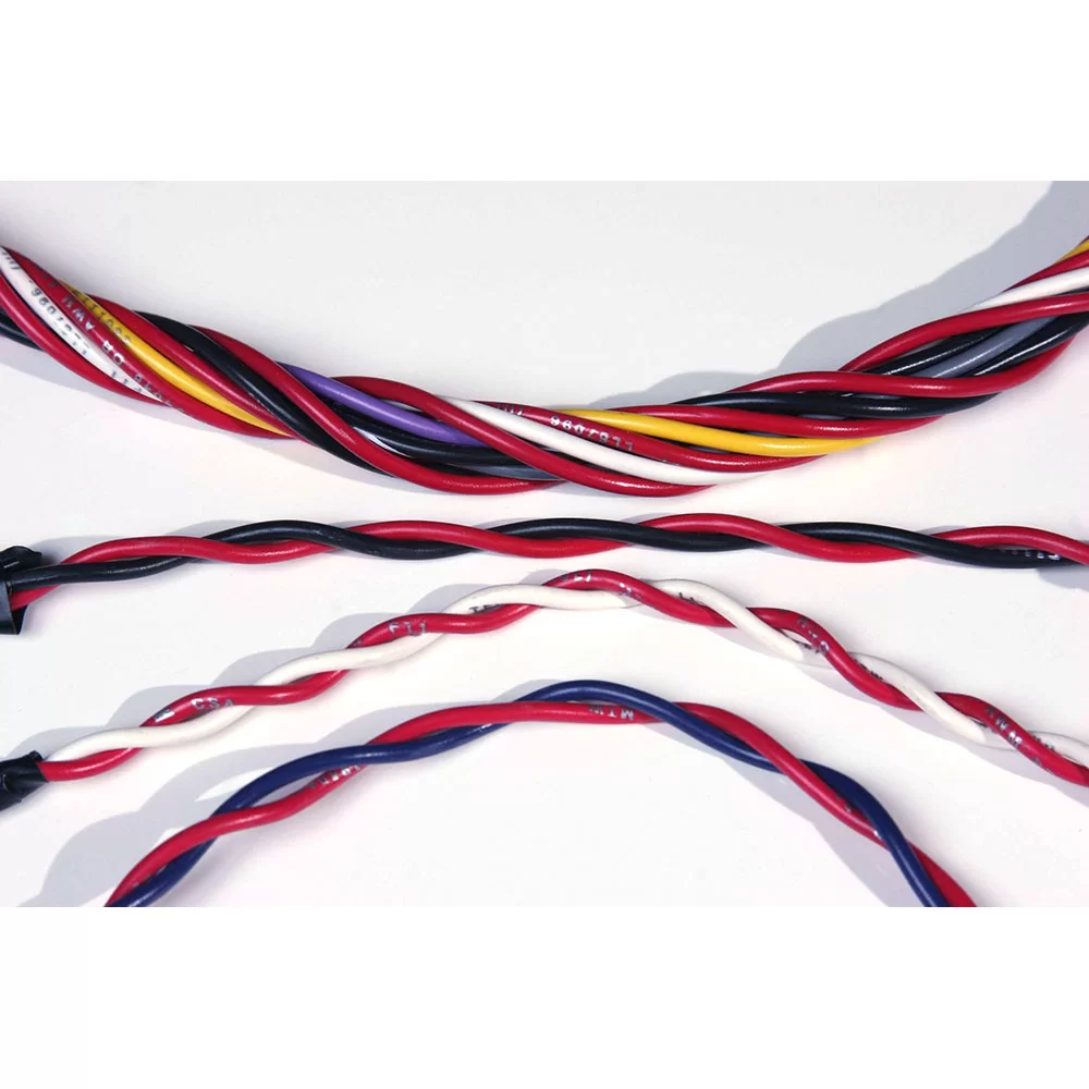
Cable Wire-harness assembly, sheet metal, Electrical cabinet Assembly service, Conformal coating, Prototyping and mass production...
We are willing to sign NDA in high confidential level.
The shipping cost is determined by the destination, weight, packing size of the goods. Please let us know if you need us to quote you the shipping cost.
As to PCBA production, there are automated optical inspection (AOI) for each batch, X-ray inspection for BGA parts, first article inspection(FAI) before mass production.
DIP (Dual In-Line Package) insert processing is a manufacturing technique used to insert through-hole components into a printed circuit board (PCB) that has pre-drilled holes. DIP components have leads or pins that extend from the bottom and are inserted through the holes in the PCB. The DIP insert processing typically involves the following steps:
1. PCB Preparation: The PCB is prepared for DIP component insertion. This involves ensuring that the PCB has pre-drilled holes in the correct locations and sizes to accommodate the DIP component leads.
2. Component Preparation: The DIP components are prepared for insertion. This may involve straightening or aligning the component leads to ensure they can be easily inserted into the PCB holes.
3. Insertion: Each DIP component is manually or automatically inserted into the corresponding holes on the PCB. The component leads are carefully aligned with the holes and inserted until the component body rests flush against the PCB surface.
4. Securing: Once the DIP components are inserted, they are secured to the PCB to ensure they remain in place during subsequent manufacturing processes and the product's lifecycle. This can be achieved through various methods, such as soldering, crimping, or using adhesive.
5. Soldering: After the DIP components are inserted and secured, the PCB is typically subjected to a soldering process to create reliable electrical connections. This can be done through wave soldering, selective soldering, or hand soldering, depending on the production setup and requirements.
6. Inspection: Once soldering is complete, the PCB undergoes inspection to verify the quality of the solder joints and component placement. Visual inspection, automated optical inspection (AOI), or other testing methods may be employed to detect any defects, misalignments, or soldering issues.
7. Testing: The assembled PCB, with the inserted and soldered DIP components, may undergo functional or electrical testing to ensure it meets the required specifications and performs as intended.
8. Final Assembly: After testing, the PCB may proceed to final assembly, where additional components and processes are added to complete the product.
DIP insert processing is commonly used for components that cannot be mounted using surface mount technology (SMT) or for applications where through-hole components are preferred due to their robustness or specific electrical requirements.
The importance of ICT automation lies in its ability to streamline the testing phase of PCB production. With the increasing complexity of electronic devices and the demand for faster production, automating PCB testing is no longer optional—it’s a necessity. By leveraging ICT automation, manufacturers can meet tight deadlines, maintain high-quality standards, and reduce costs associated with defective products.
For industries where precision and reliability are paramount—such as aerospace, medical devices, and automotive—ICT automation is not just a tool; it’s a strategic asset. It enables manufacturers to deliver flawless products to customers, build trust, and maintain a strong reputation in the market.
Electronic Design Services
PCB and Schematic reviews
Complete electronic design partners available
Design For Manufacture
Product Lifecycle Management
PCB Assembly
Fast turnaround of PCB fab, stencils and PCB assembly
BOM in one box service, turnkey PCBA for whole board delivery
Leaded, lead-free, RoHS, through-hole, SMT capability
Final Assembly & Test
Conformal Coating, potting
Plastic molding, sheet metal
Painting, powder coating
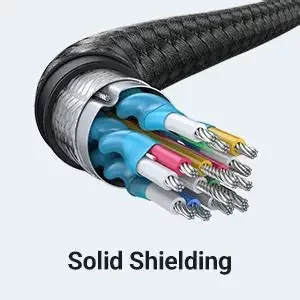
Cable assembly - Data, Power, RF & Optical
Automated Production Test
Main Business:
Software supporting (function testing, firmware install, chip burning)
PCBA data (PCB file, BOM list, SCH schematic diagram)
PCBA sample preparation (PCB production, material procurement, SMT processing, PCBA Prototype, PCBA debugging)
PCBA batch (PCBA medium and small batch)
PCBA after-sales service (PCBA warranty, PCBA Clone, OEM, Reverse engineering, IC cracking)
What is of most importance is how the material behaves at temperatures above the Tg value (post Tg) so knowing the temperature profiles the board will be subjected to will help you look evaluate the necessary performance characteristics.

