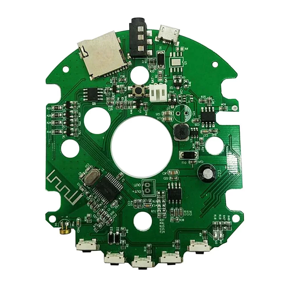
1. Features: Miniaturized, low power consumption, highly integrated, with wireless communication capability.
2. Applications: Smart home, wearable devices, intelligent transportation, and other IoT fields.
3. Selling Points: Uses advanced low-power chips and wireless communication modules, miniaturized design and high-density assembly processes, with good compatibility and expandability.
4. Processes: SMT and micro-packaging technologies, AOI test, FT test, ICT test, BGA technic, selective wave soldering, SMT, DIP, wave soldering, reflow soldering
5. Customization: customization according to customers' design files.
6. ISO 9001:2015+ AS9100D Certified

PCBA(printed circuit board assembly) can perform more powerful functions than bare PCB (printed circuit board) and support the operation of robots.

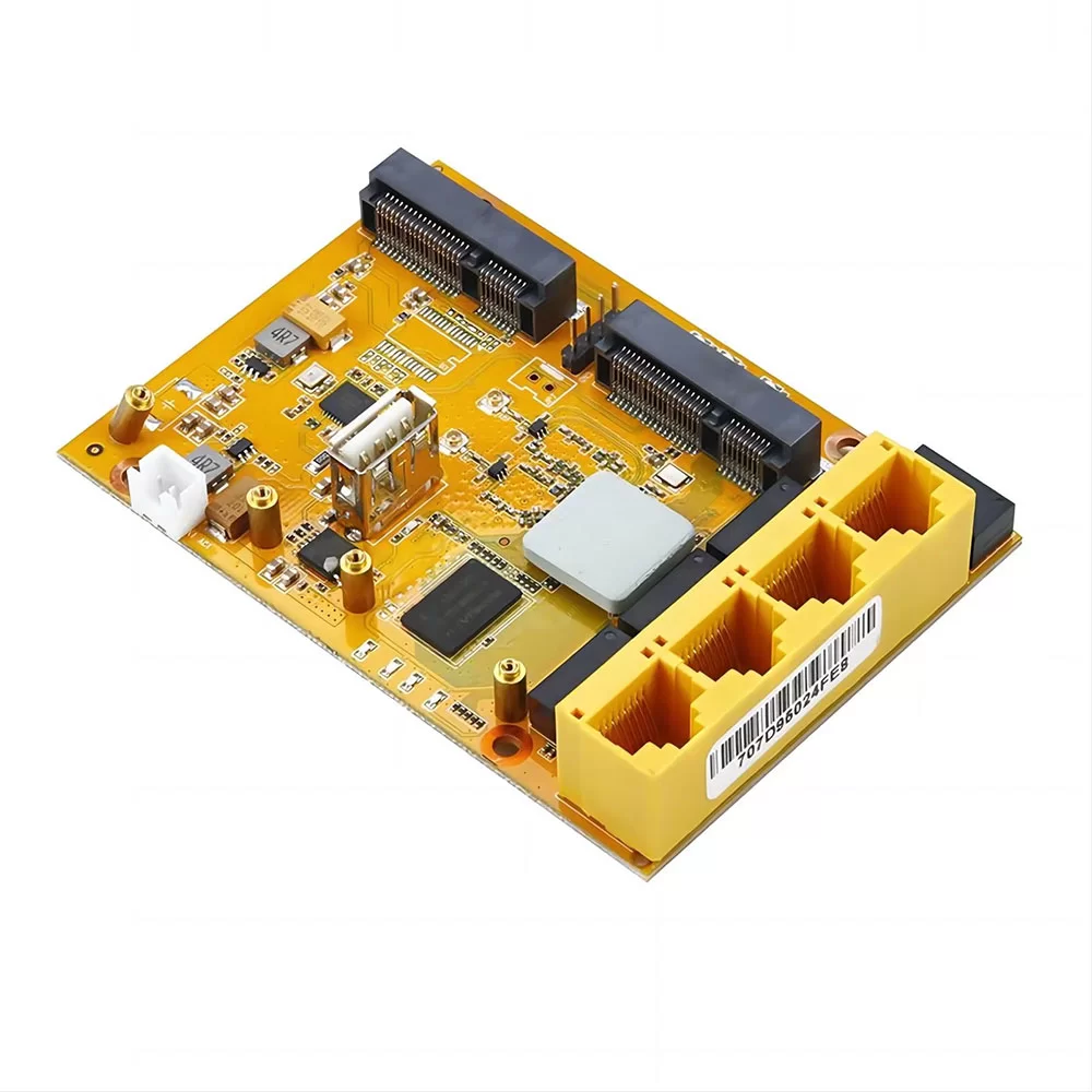
Hardware Platform: All router functions rely on the PCBA board as the hardware platform.

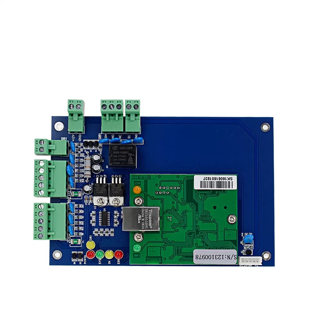
These assemblies comprise specialized control boards designed to manage, monitor, and restrict access to specific resources or areas.

The main differences between PCB assembly for programming education boards and other general PCB assemblies lie in design goals, component types, assembly processes, and application scenarios.

Internet of Things (IoT) refers to various devices and technologies such as various information sensors, radio frequency identification technology, global positioning system, infrared sensor, laser scanner, etc. Objects or processes collect a variety of information, light, heat, electricity, mechanics, chemistry, biology, location and other needs.


