Specification (or material number): | Material specific parameters (mm): | Pad design (mm): | Printed tin stencil design: | Notes: |
QFP |
|
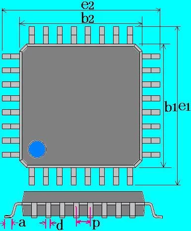
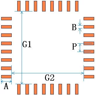
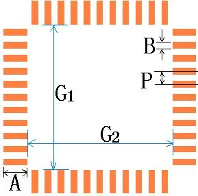
A=a+0.8,B=0.19mm P=p G1=e1-2*(0.4+a) G2=e2-2*(0.4+a) |
| The pin length is changed from a+0.70mm to a+0.80mm, which is good for repair and printed pull tip handling. For the height of 3.8mm LQFP pad design width is used 0.23mm (stencil opening width 0.19mm) |
QFP |
|
A=a+0.7,B=0.17mm P=p G1=e1-2*(0.4+a) G2=e2-2*(0.4+a)
| T=0.10mm. Pin opening width 0.15mm |
|
PLCC |
|
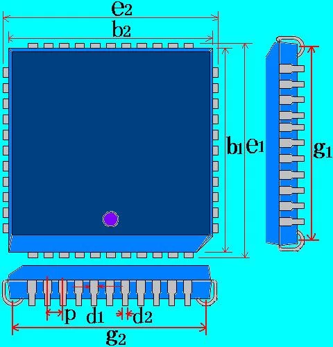
A=1.8mm,B=d2+0.10mm G1=g1-1.0mm, G2=g2-1.0mm, P=p |
|
|
BGA |
|
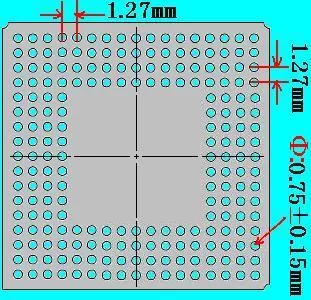
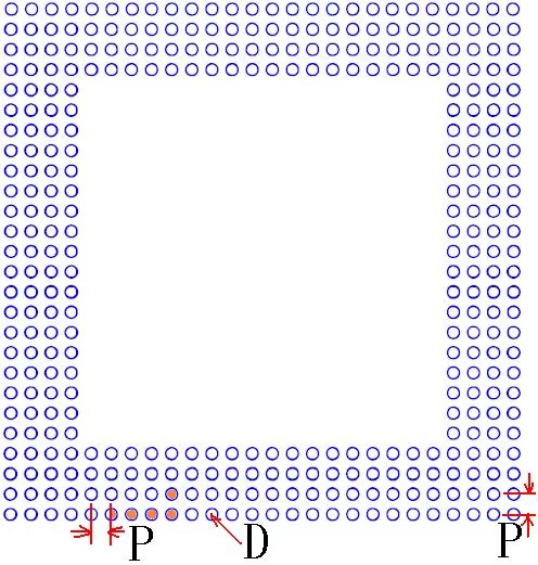
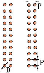
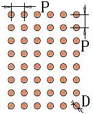
D=0.70mm P=1.27mm
| Recommended stencil opening diameter is 0.75mm | Does not represent the arrangement of the actual BGA bottom solder balls |
BGA |
|
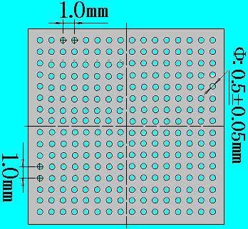
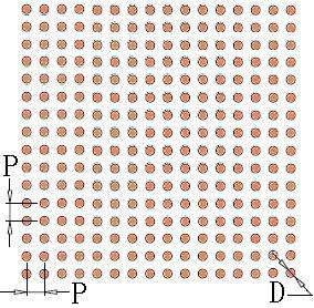
D=0.45mm P=1.00mm | Recommended stencil opening diameter is 0.50mm | Does not represent the arrangement of the actual BGA bottom solder balls |
BGA |
|
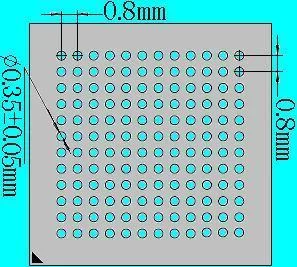
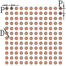
D=0.35mm P=0.80mm
| Recommended stencil opening diameter is 0.40mm | Does not represent the arrangement of the actual BGA bottom solder balls |
BGA |
|
D=0.40mm P=0.80mm | Recommended stencil opening diameter is 0.40mm | Does not represent the arrangement of the actual BGA bottom solder balls |
BGA |
|
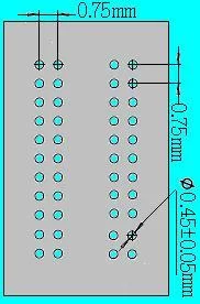
D=0.3mm P=0.75mm | Recommended stencil opening diameter is 0.40mm | Does not represent the arrangement of the actual BGA bottom solder balls |
BGA |
|
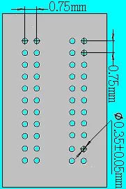
D=0.3mm P=0.75mm | Recommended stencil opening diameter is 0.35mm | Does not represent the arrangement of the actual BGA bottom solder balls |
LGA (Ball-less BGA) |
|
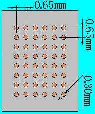
D=0.3mm, P=0.65mm | Recommended stencil 1:1 opening | Does not represent the arrangement of the actual BGA bottom solder balls |
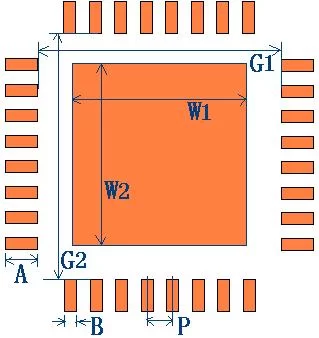
QFN |
|
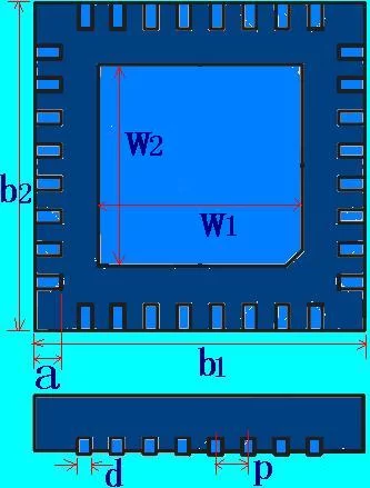
A=a+0.35,B=d+0.05 P=p,W1=w1,W2=w2 G1=b1-2*(0.05+a) G2=b2-2*(0.05+a)
Design independent pads for each pin. Note: If the ground pad to design the thermal over-hole, it should be 1.0mm-1.2mm gap evenly distributed in the central thermal pad, over-hole should be connected to the PCB inner metal ground layer, over-hole diameter recommended for 0.3mm-0.33mm | It is recommended that the stencil pin opening length direction flare 0.30mm, ground pad opening bridge, bridge width 0.5mm, the number of bridges W1/2, W2/2, take the integer.
If the pad design has holes, stencil openings to avoid holes, grounding pad opening area of 50% to 80% of the grounding pad area can be, too much tin on the pin welding has a certain impact |
|
QFN | A=a+0.3,B=d, P=p W1=w1,W2=w2 G1=b1-2*(0.05+a) G2=b2-2*(0.05+a) | It is recommended to flare 0.20mm in the direction of the stencil pin opening length, and the rest as described above |
| |
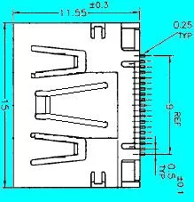
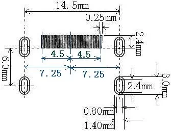
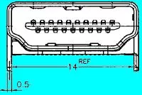
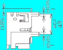
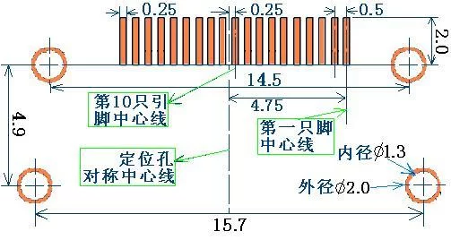
HDMI |
|
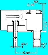
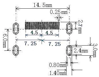
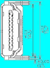
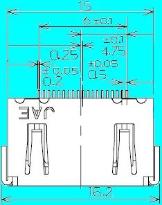
| It is recommended that the stencil opening pin width in accordance with 0.27mm opening, pin length direction outward expansion 0.3mm opening |
|
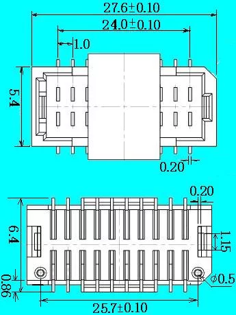
HDMI |
|
| It is recommended that the stencil opening pin width in accordance with 0.27mm opening, pin length direction outward expansion 0.3mm opening | When trial production pay attention to see if the size design is suitable |
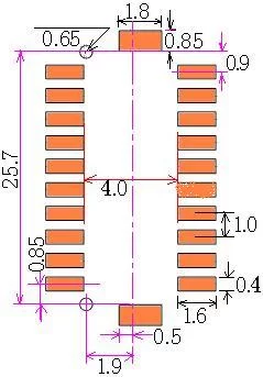
HDMI |
|
| It is recommended that the stencil opening pin width in accordance with 0.265mm opening, pin length direction outward expansion 0.3mm opening |
|
5400-997000-50 |
|
| It is recommended that the stencil pins be opened at 0.6mm in width and 0.4mm outward in the direction of the pin length. |
|

