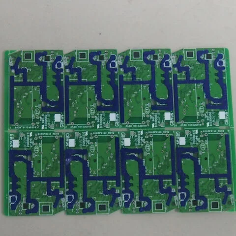
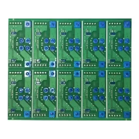
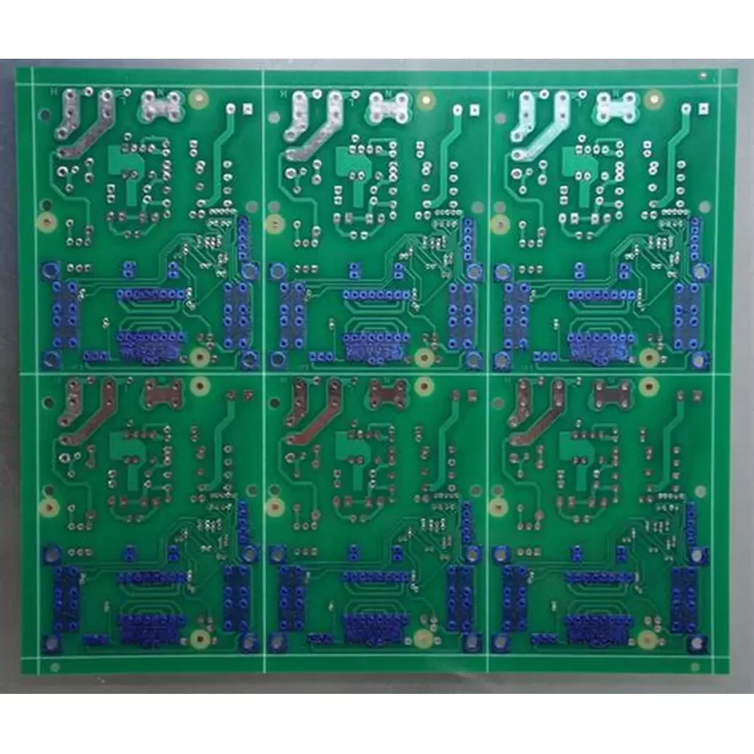
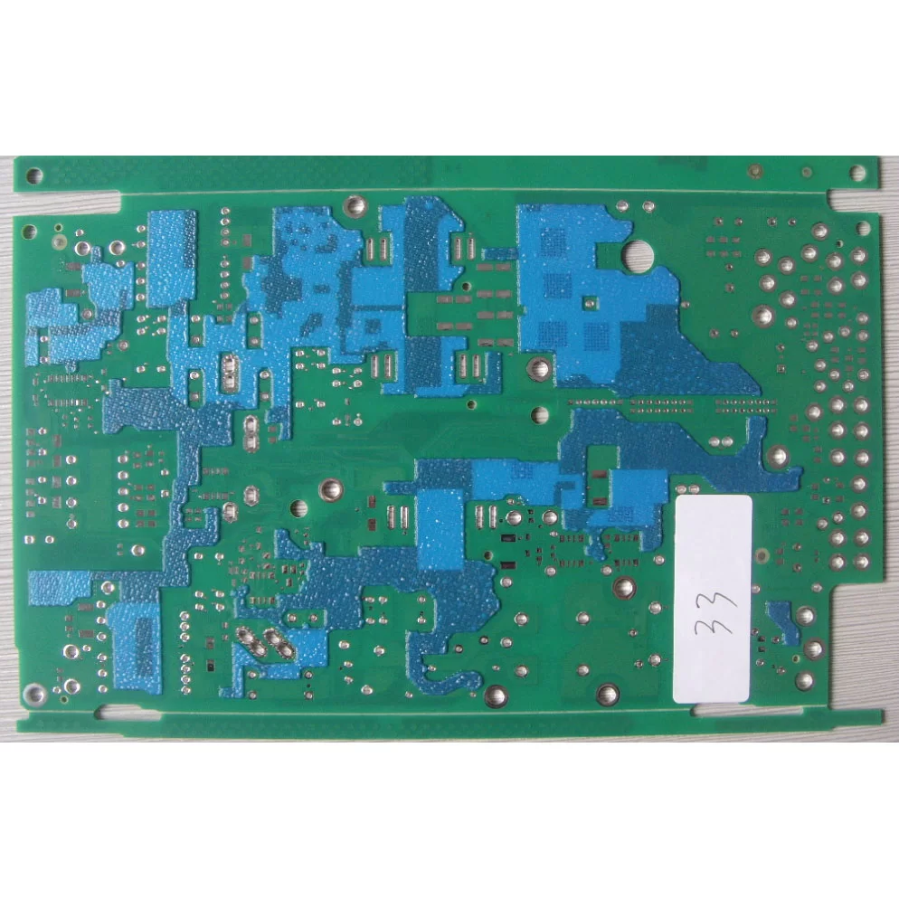
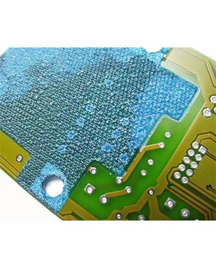
Blue Peelable Printed Circuit Boards
What is a Peelable Solder Mask?
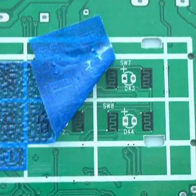
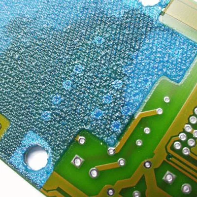
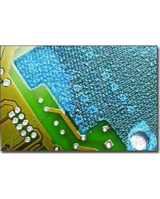
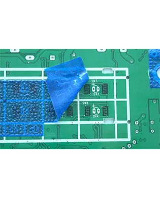
A peelable solder mask is a temporary protective coating applied to specific areas of a PCB during the manufacturing process. Unlike traditional permanent solder masks, peelable masks are designed to be easily removed after serving their protective purpose.
Key Features of Peelable Solder Masks:
Temporary protection for PCB surfaces
Easy application and removal
Resistant to high temperatures and chemicals
Prevents solder bridging and component misalignment
Leaves no residue upon removal
Peelable solder masks act as a shield, safeguarding critical areas of the PCB from damage, contamination, and unwanted solder during various stages of the assembly process.
Why Use Peelable Solder Masks in PCB Manufacturing?
The adoption of peelable solder masks in PCB manufacturing has grown significantly due to the numerous benefits they offer. Let’s explore the key advantages that make peelable solder masks an essential tool in modern electronics production.
1. Precision Protection
Peelable solder masks allow manufacturers to selectively protect specific areas of the PCB, ensuring that only intended areas are exposed to soldering processes. This precision is crucial for:
Preventing solder bridges between closely spaced components
Protecting delicate surface-mount pads
Safeguarding plated through-holes from solder ingress
2. Enhanced Quality Control
By using peelable solder masks, manufacturers can:
Reduce defects caused by excess solder
Minimize component misalignment issues
Improve overall PCB assembly quality
3. Cost-Effective Solution
Implementing peelable solder masks in the PCB assembly process can lead to significant cost savings:
Reduced rework and repair costs
Fewer scrapped boards due to assembly errors
Increased production efficiency
4. Versatility in Manufacturing Processes
Peelable solder masks are compatible with various PCB manufacturing and assembly techniques, including:
Wave soldering
Reflow soldering
Selective soldering
Hand soldering
5. Environmental Considerations
Many peelable solder mask formulations are environmentally friendly, offering:
Low volatile organic compound (VOC) emissions
Easy disposal without harmful residues
Compliance with RoHS and REACH regulations
Types of Peelable Solder Masks
Peelable solder masks come in various types, each designed to meet specific manufacturing requirements and PCB designs. Understanding these types can help in selecting the most appropriate mask for a given application.
1. Liquid Peelable Solder Masks
Liquid peelable masks are applied in a liquid form and then cured to create a protective layer.
Advantages:
Can be easily applied using screen printing or spraying techniques
Excellent conformity to PCB surface contours
Suitable for both small and large areas of coverage
Applications:
High-volume PCB production
Complex PCB layouts with varying surface topographies
2. Film-Based Peelable Solder Masks
These masks come in the form of pre-cut films that are applied to the PCB surface.
Advantages:
Quick and easy application
Uniform thickness across the protected area
Ideal for protecting large, flat areas of the PCB
Applications:
Batch production of PCBs with similar designs
Protection of entire PCB sides during double-sided assembly
3. Heat-Resistant Peelable Solder Masks
Specially formulated to withstand high temperatures encountered in soldering processes.
Advantages:
Can withstand temperatures up to 300°C or higher
Excellent protection during reflow and wave soldering
Maintains integrity through multiple heat cycles
Applications:
High-temperature soldering processes
Multi-layer PCB assembly with multiple reflow cycles
4. Chemical-Resistant Peelable Solder Masks
These masks offer protection against various chemicals used in PCB manufacturing.
Advantages:
Resistant to flux, cleaning solvents, and other PCB chemicals
Maintains integrity during chemical processes
Prevents chemical ingress into protected areas
Applications:
PCBs undergoing chemical cleaning processes
Boards exposed to harsh environmental conditions
If you have any camping barbeque equipment inquiry, please feel free to contact us.
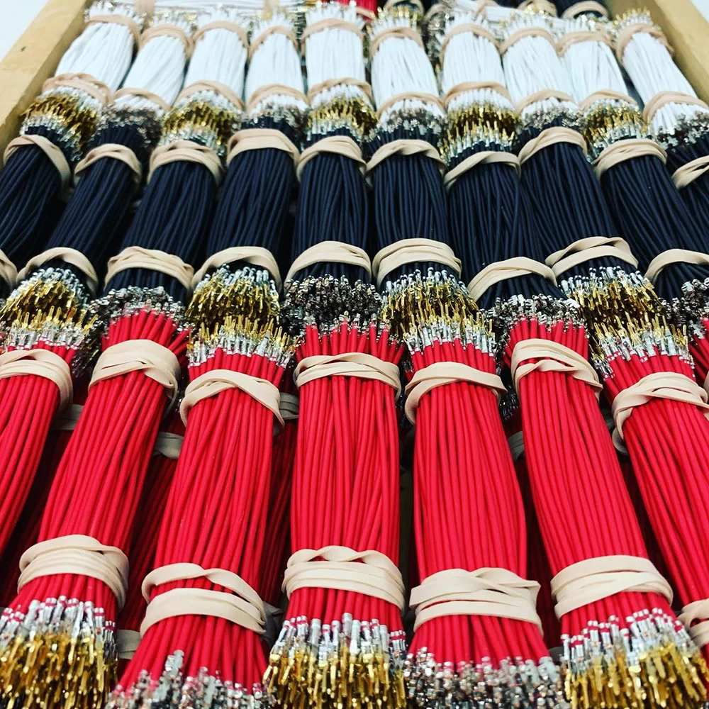
Managing kitting and packaging in-house can be time-consuming, costly, and error-prone.
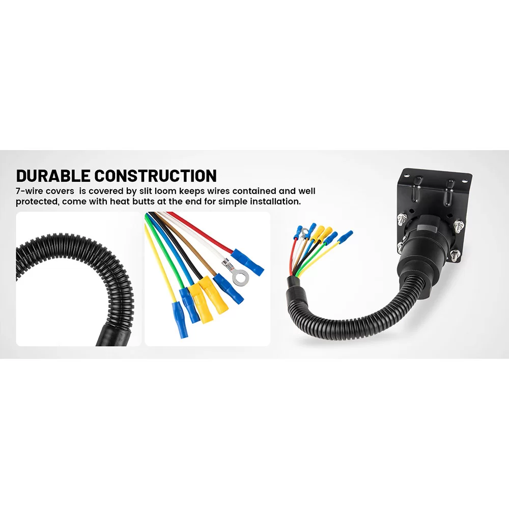
Maybe an off-the-shelf cable can't meet your needs.
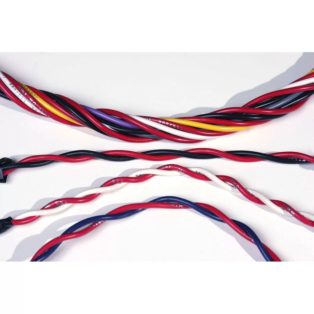
Twisting entwines multiple wires and arranges them tightly next to each other. Depending on the AWG size, we can group up to fifty conductors.
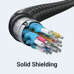
Shielding refers to the metallic layer surrounding a cable’s conductor, created to limit signal interference between the wire and external fields.
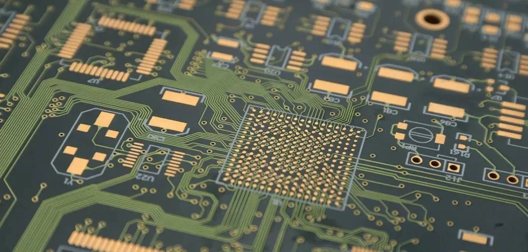
PCB manufacturing is the process of building a physical PCB from a PCB design according to a certain set of specifications.

The following design standards refer to the IPC-SM-782A standard and the design of some famous Japanese design manufacturers and some better design solutions accumulated in the manufacturing experience.
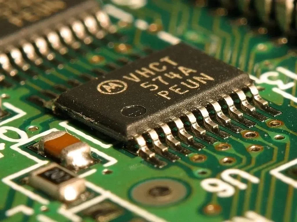
Via holes, also known as through holes, play a role in connecting different parts of a circuit board.

