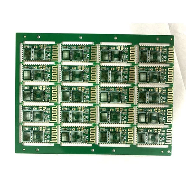
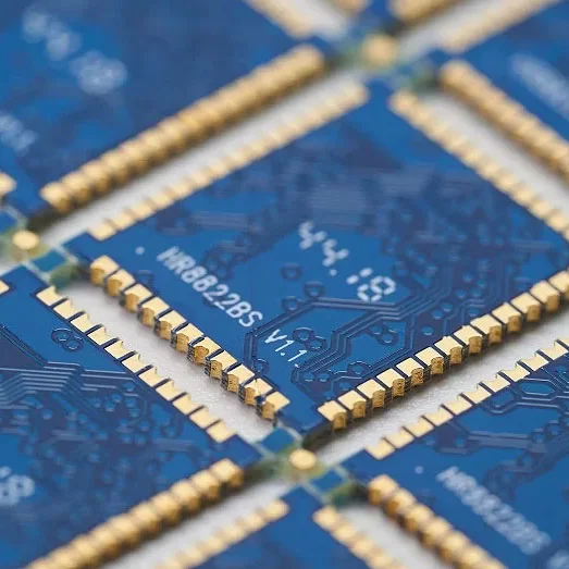
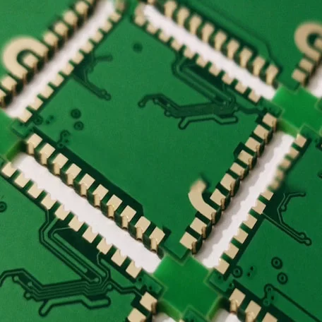
Half hole WiFi Module PCB
Parameter
Model: Half hole WiFi Module PCB
Material: FR4
Layer: 4Layers
Color: Black/White
Finished Thickness: 1.0mm
Copper Thickness: 1OZ
Surface Treatment: Immersion Gold
Min Trace: 4mil(.1mm)
Min Space: 4mil(0.1mm)
Characteristic: Half hole PCB
Application: WiFi module
What‘s Half hole PCB?
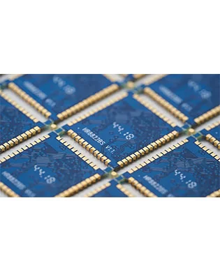
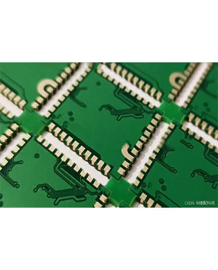
The half-hole Wi-Fi module PCB is the core circuit board for Wi-Fi modules. Half-holes are typically designed at the extreme edge of the PCB; half the hole is removed during routing, leaving the remaining half as a "half-hole".
The key lies in the edge "half-hole process"—precisely controlling half-hole depth, hole copper uniformity, and board-splitting stress. This ensures the edge half-holes enable miniaturization (50% less space than traditional connectors), stable 2.4G/5G high-frequency Wi-Fi transmission, and far better vibration resistance than standard interfaces.
Most modular PCBs adopt half-holes for easy soldering, small module size, and multiple functional requirements.
Benefits
Ultra-Optimized Space
Half-holes replace traditional connectors, reducing module thickness by 60% for a smaller overall size and meeting miniaturization design needs.
Stronger Connection Stability
Welding strength far exceeds plug-in interfaces, with enhanced vibration resistance, lower contact resistance, and more stable signal transmission.
Signal Transmission Integrity
Half-holes can be directly soldered to external antennas (e.g., ceramic antennas) or seamlessly connect to motherboard RF lines via board-edge half-holes, optimizing signal integrity.
Applications of Half-Hole PCBs
Consumer Electronics: Used in motherboards for mobile phones, tablets, and TVs, as well as power supply, communication, and display modules. Its design enhances circuit connection and signal transmission, boosting product performance and stability.
- Automotive Electronics: Applied in automotive electronic control units (ECUs) like engine and body control units. Its high reliability and stability ensure normal operation of automotive electronic systems, improving vehicle safety and performance.
- Industrial Control: Used in control circuit boards for industrial automation equipment, including PLCs, frequency converters, and servo drivers. Its high-density wiring and stability meet signal transmission and circuit connection requirements, enhancing equipment accuracy and reliability.
- Medical Equipment: Applied in control circuit boards for medical devices such as ECG machines, blood pressure monitors, and ventilators. Its high precision and stability ensure device accuracy and reliability, improving medical diagnosis and treatment effects.
If you have any camping barbeque equipment inquiry, please feel free to contact us.
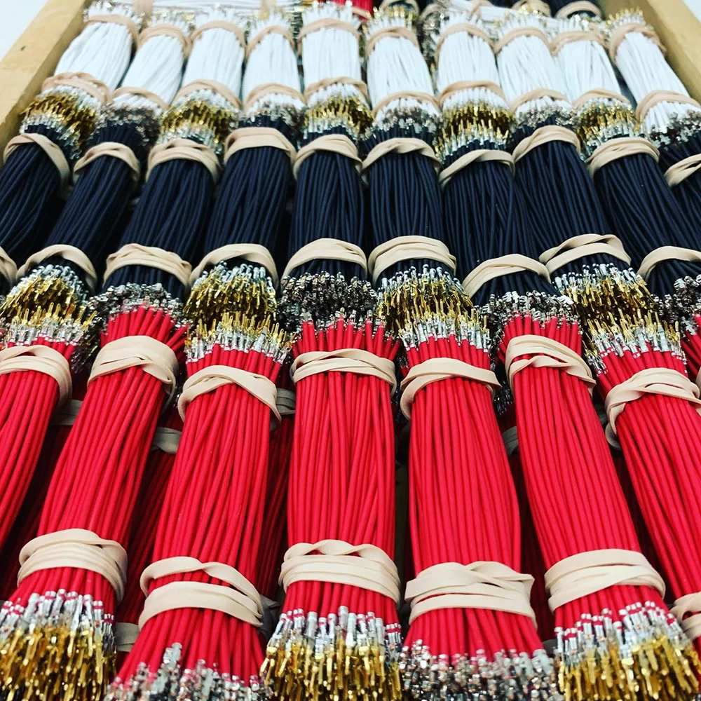
Managing kitting and packaging in-house can be time-consuming, costly, and error-prone.
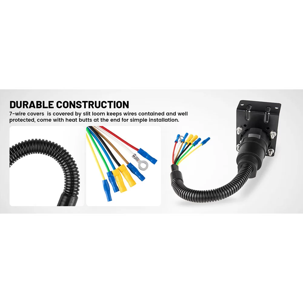
Maybe an off-the-shelf cable can't meet your needs.
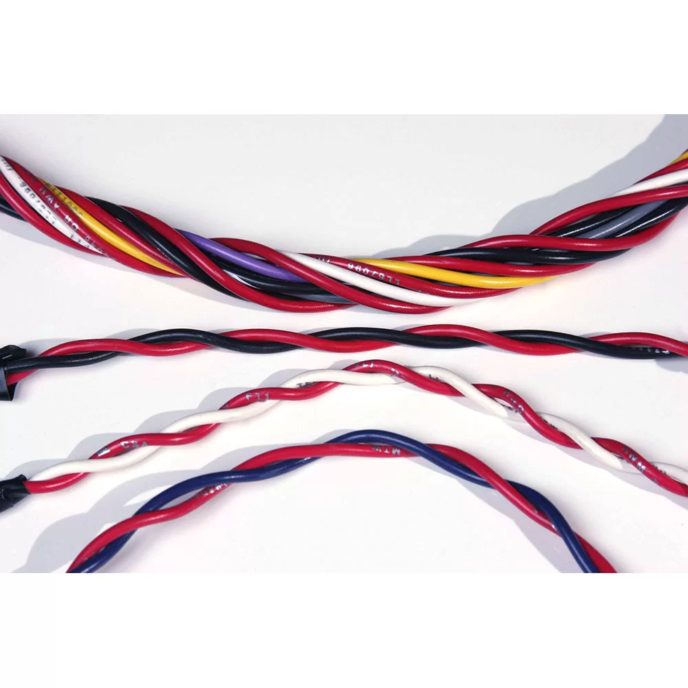
Twisting entwines multiple wires and arranges them tightly next to each other. Depending on the AWG size, we can group up to fifty conductors.
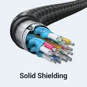
Shielding refers to the metallic layer surrounding a cable’s conductor, created to limit signal interference between the wire and external fields.
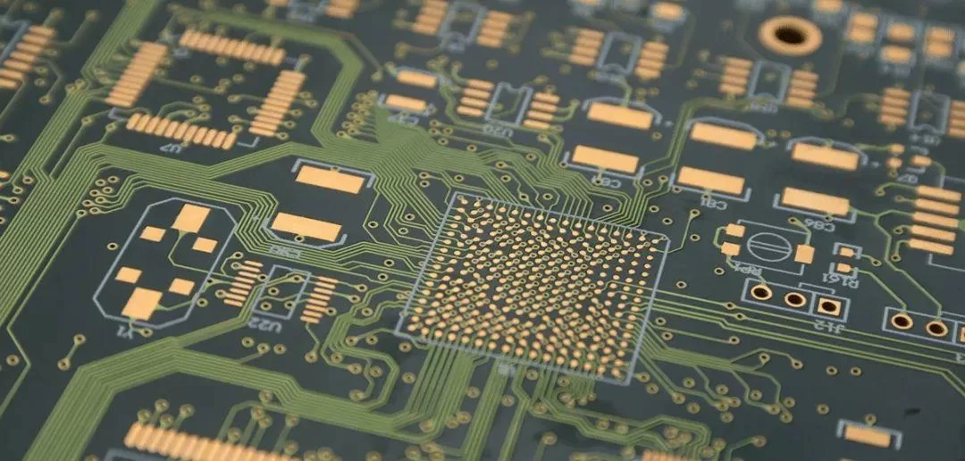
PCB manufacturing is the process of building a physical PCB from a PCB design according to a certain set of specifications.

The following design standards refer to the IPC-SM-782A standard and the design of some famous Japanese design manufacturers and some better design solutions accumulated in the manufacturing experience.
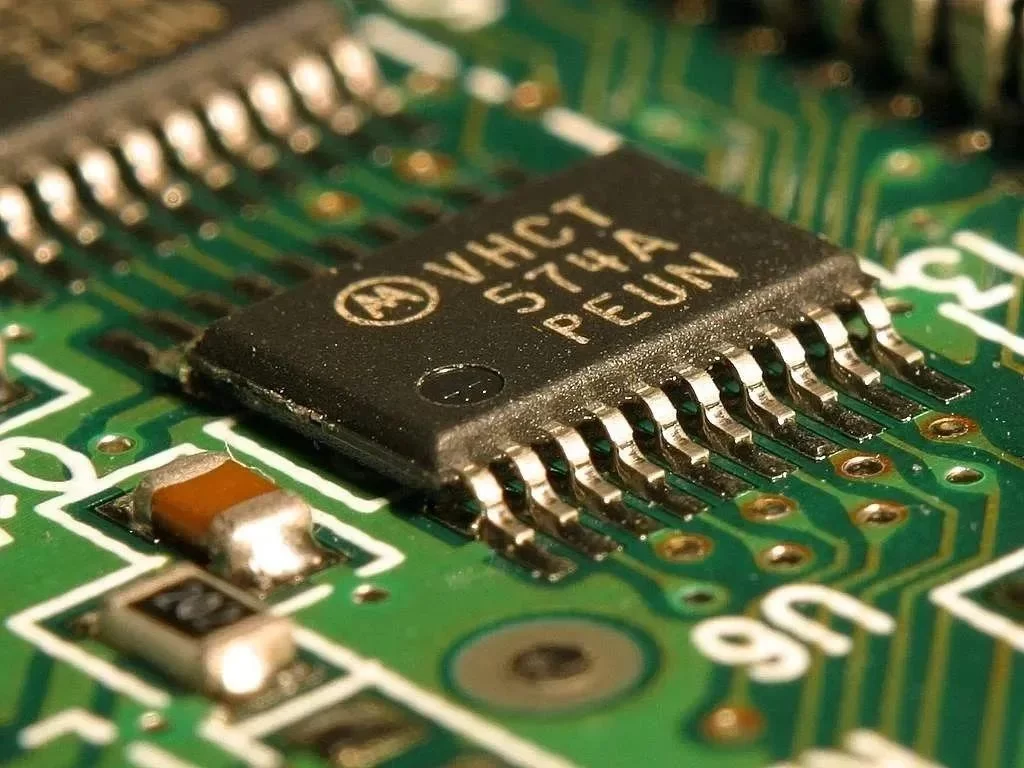
Via holes, also known as through holes, play a role in connecting different parts of a circuit board.

