HDI Printed Circuit Boards (PCB)
Data Sheet
Model: HDI PCB
Layers: 4 layer -48 layer
- Material: Shengyi, Tuc,ITEQ, Panasonic
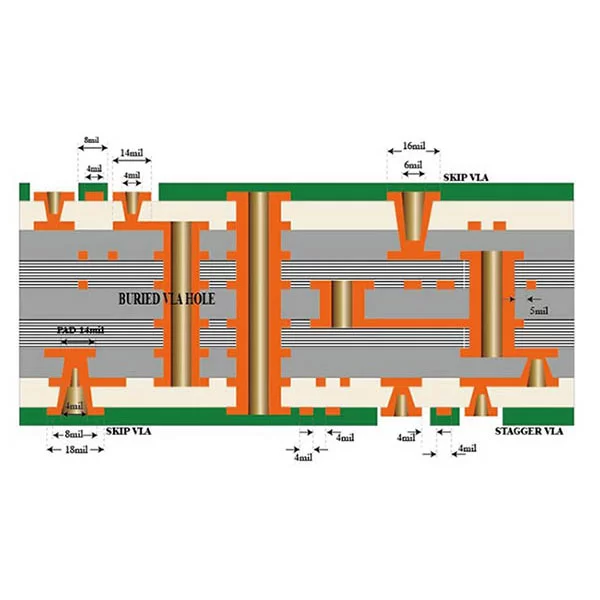
- Construction:1-5N, anylayer HDI PCB
- Finished Thickness:0.3-3.2mm
- Copper Thickness: 0.5OZ/1OZ
- Color: Green/White/Black/Red/Blue
- Surface treatment: ENIG/OSP
- Special technology: Gold thickness
- Min Trace/ Space:BGA 2mil/2mil
What's HDI PCB?
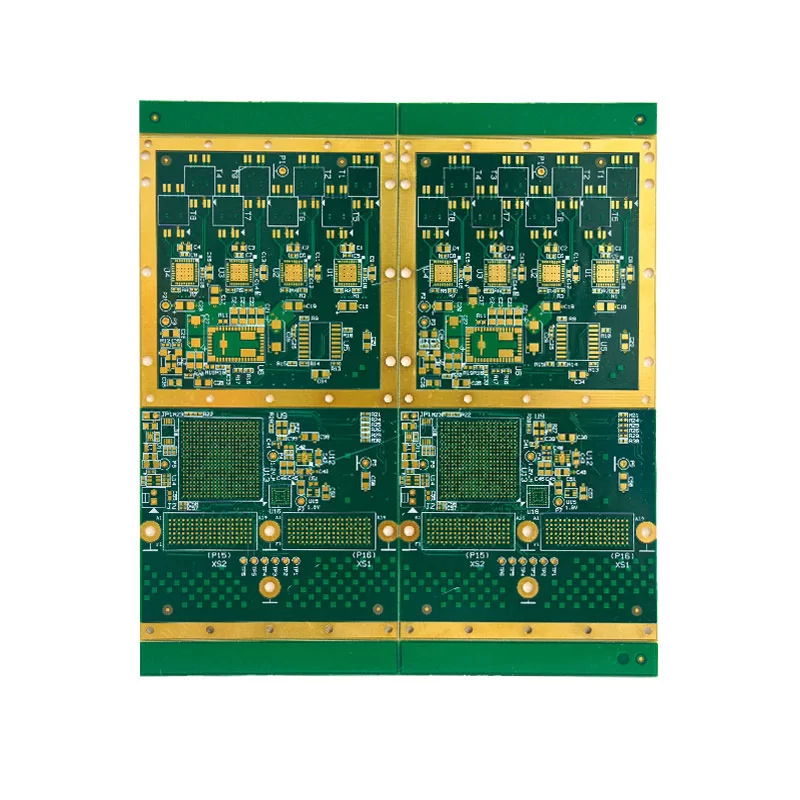
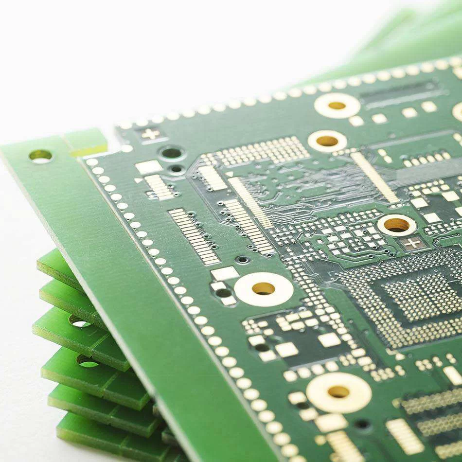
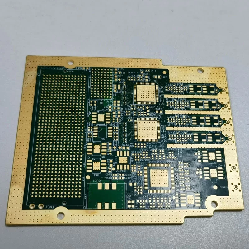
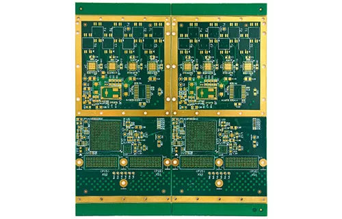
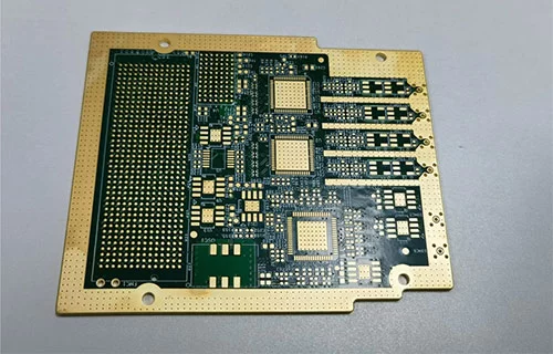
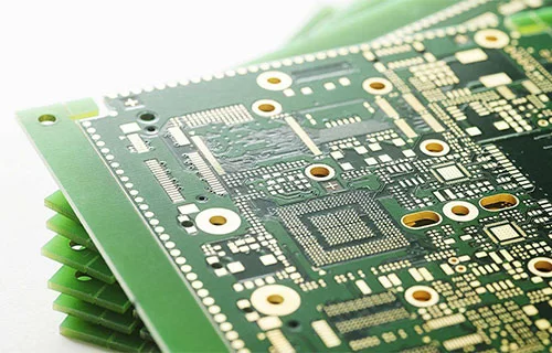
High-Density Interconnect (HDI) Printed Circuit boards are multilayer boards with high-density wiring per unit area. These PCBs function to distribute the signal while being small in size. The dense placement of wire components and pins in small parts ensures they take up less space, making the electronics more compact. They can be used in high-performance electronics such as IoT devices, wearables, and smartphones.
Advantages
Miniaturization: Using HDI in smartphones, watches, and other devices can reduce the motherboard area by 25%, freeing up space for components like batteries.
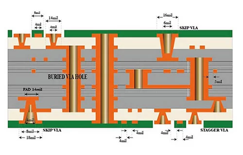
Improving signal performance: Microvias shorten transmission distances, improving signal integrity by 40% in 5G base station HDI boards, with a packet loss rate of ≤ 0.1%.
- Reducing costs and weight: 6-layer HDI can replace traditional 8-layer boards, reducing costs by 15% and weight by 20%, extending drone flight time by 10 minutes.
Applications
Commercial Products, mobile phones, tablets, smartwatches, Cameras, Automotive, Virtual Reality devices operate, Defense and Aerospace, and supercomputer systems like space stations, Healthcare and Medical Devices, high precision small cameras, robotic arm, precise laser operating machines
Key Process Points
1. Laser drilling accuracy ≤ ±0.01mm;
- 2. Lamination positioning error ≤ ±5μm to avoid blind via misalignment;
- 3. Microvia copper layer thickness ≥ 20μm, using combined X-ray and AOI inspection to ensure quality.
HDI is a key area of PCB technology advancement, enabling electronic devices to achieve high performance in a compact form factor. With the development of technologies like 5G and AI, HDI applications will become increasingly widespread.
Challenges
PCB area is small
Smaller components and tightly packed arrangements
- Both sides of the PCB have a large number of components
- The trace length is long and the delay time is more
- More complex routing and more nets in routing are required
If you have any camping barbeque equipment inquiry, please feel free to contact us.
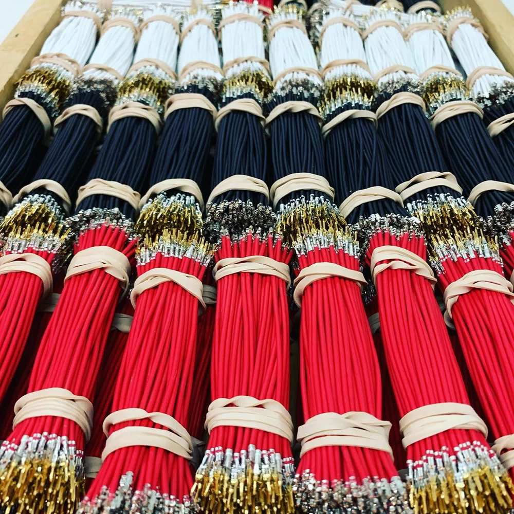
Managing kitting and packaging in-house can be time-consuming, costly, and error-prone.
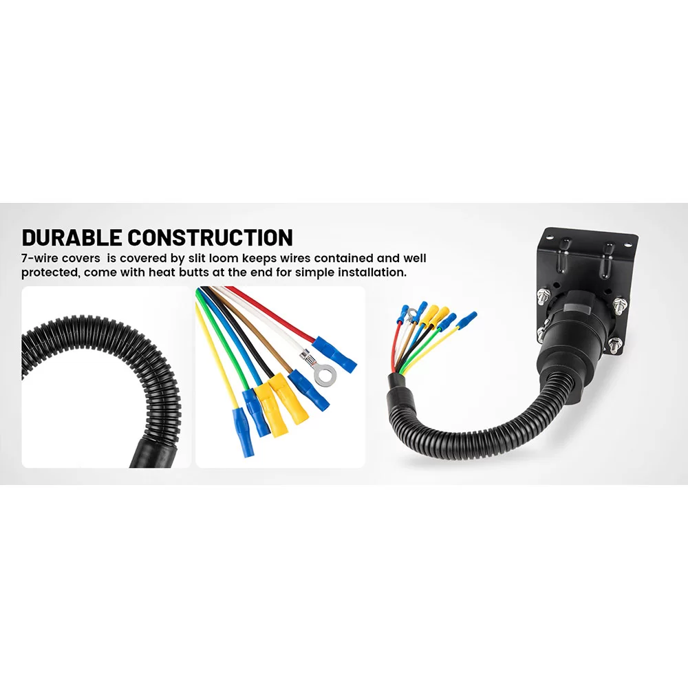
Maybe an off-the-shelf cable can't meet your needs.
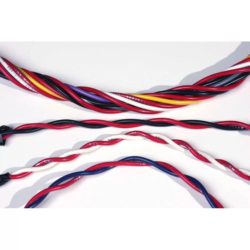
Twisting entwines multiple wires and arranges them tightly next to each other. Depending on the AWG size, we can group up to fifty conductors.
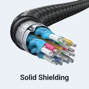
Shielding refers to the metallic layer surrounding a cable’s conductor, created to limit signal interference between the wire and external fields.
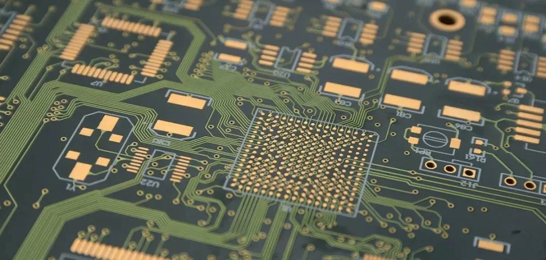
PCB manufacturing is the process of building a physical PCB from a PCB design according to a certain set of specifications.

The following design standards refer to the IPC-SM-782A standard and the design of some famous Japanese design manufacturers and some better design solutions accumulated in the manufacturing experience.
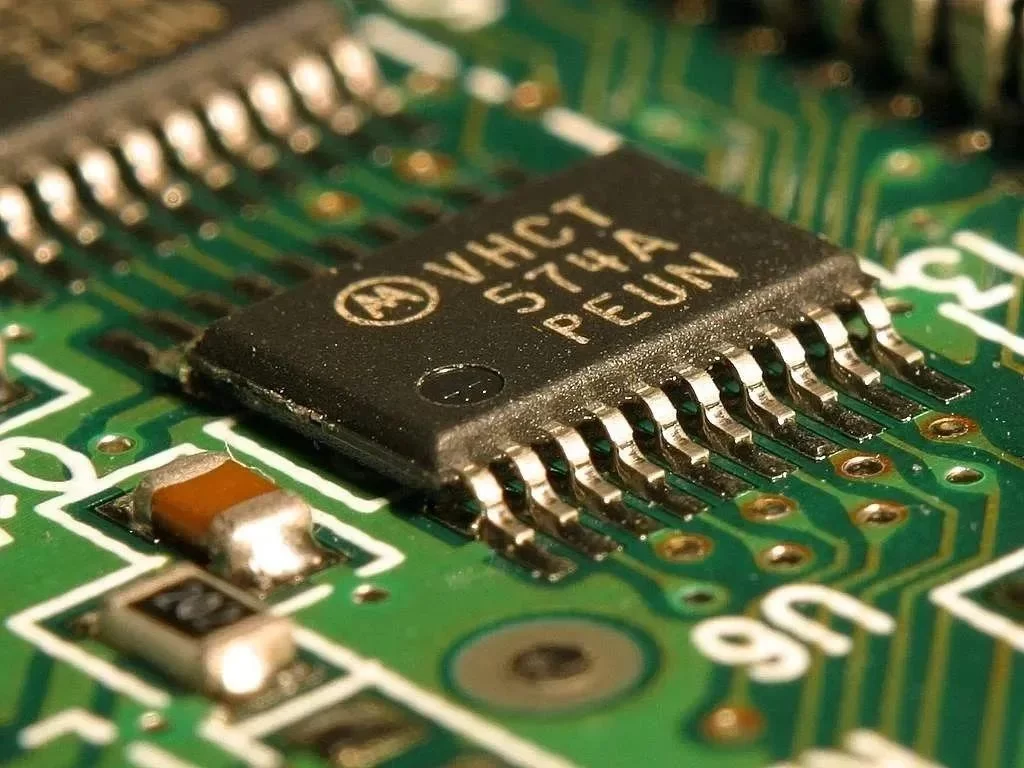
Via holes, also known as through holes, play a role in connecting different parts of a circuit board.

