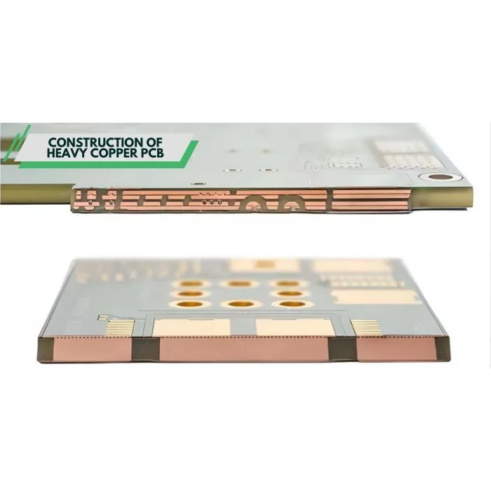
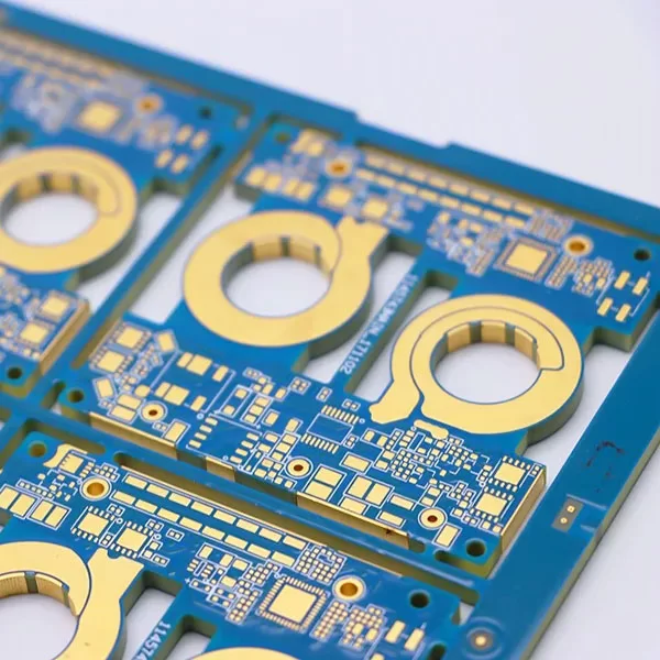
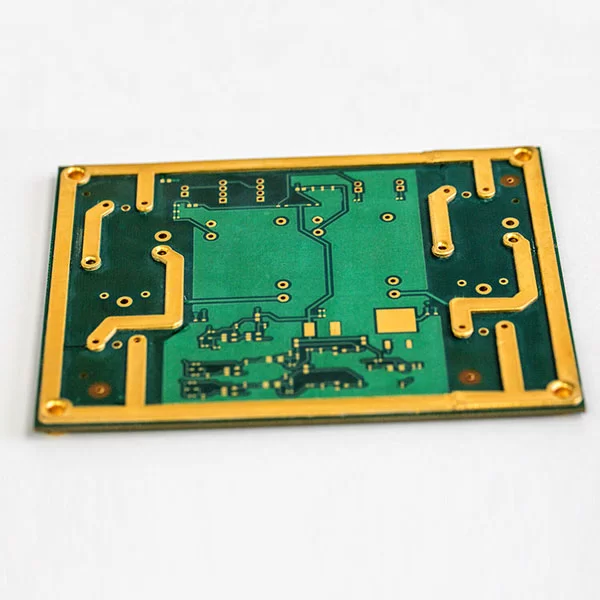
Heavy Copper PCB
Datasheet
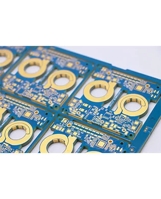
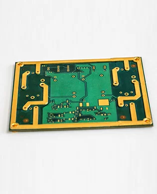
Model: Heavy Copper PCB
PCB Material: SY
PCB Layer: 6Layers
Soldermask Color: Green
Silk Screen: White
Copper thickness: 2OZ/6OZ(70um)
Board Thickness: 2.8mmmm
Surface technology: Immersion Gold(1-3U)
Application: Power converter Heavy Copper PCB
What is heavy copper PCBs?
Most heavy copper PCBs are made of FR4 material, but can also be made by polyimide which is called heavy copper flex PCB.The PCB copper thickness in normal PCB is around 0.5 to 2 ounces, which is 17.5 to 70um. Some printed circuit boards need thicker copper thickness than 2 ounces (70um). When the finished thickness of copper foil on the copper layer is more than 2 ounces (70um), we call it heavy copper PCB, also extreme copper PCB.
Applications
Due to their unique properties, heavy Copper PCB are widely used in a variety of fields.
The following are their main applications:
1. Power Supplies: Power supplies are essential components of electronic devices, requiring them to withstand high currents and power. Heavy Copper PCBs' high conductivity and load-carrying capacity make them an ideal choice for power supplies.
2. Industrial Control Equipment: Industrial control equipment often requires the control and monitoring of numerous sensors and actuators. Heavy Copper PCBs provide stable and reliable circuit connections, ensuring the proper functioning of these devices.
3. New Energy Vehicles: Key components in new energy vehicles, such as motor controllers and battery management systems, must withstand high current and power loads. The high performance of Heavy Copper PCBs meets these stringent requirements.
Advantages of Heavy Copper PCB
1. High Conductivity: Heavy Copper PCB utilize a thicker copper layer for enhanced conductivity, ensuring stable circuit operation.
2. Strong Load-Carrying Capacity: Heavy Copper PCB offer a high load-carrying capacity, making them suitable for high-power, high-current electronic devices and meeting the load-carrying requirements of these devices.
3. Excellent Heat Dissipation: The Heavy Copper layer provides improved heat dissipation, effectively reducing heat generated by electronic devices during operation and extending their lifespan.
4. High Reliability: The Heavy Copper PCB process undergoes rigorous quality control, ensuring the stability and reliability of the PCB and reducing equipment failure rates.
Key Technologies in Heavy Copper PCB Manufacturing
- 1. Copper Foil Lamination: Laminating the copper foil to the substrate is a key technology in heavy copper PCB manufacturing. Proper lamination temperature and pressure are crucial to ensure a tight bond between the foil and the substrate while minimizing deformation and warping.
- 2. Circuit Pattern Production: High-precision etching or engraving equipment is required to create the circuit pattern for heavy copper PCBs.
If you have any camping barbeque equipment inquiry, please feel free to contact us.
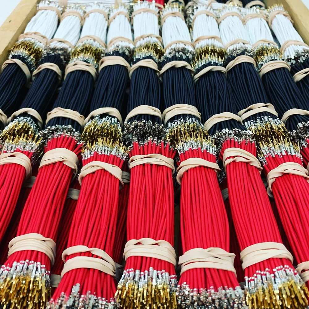
Managing kitting and packaging in-house can be time-consuming, costly, and error-prone.
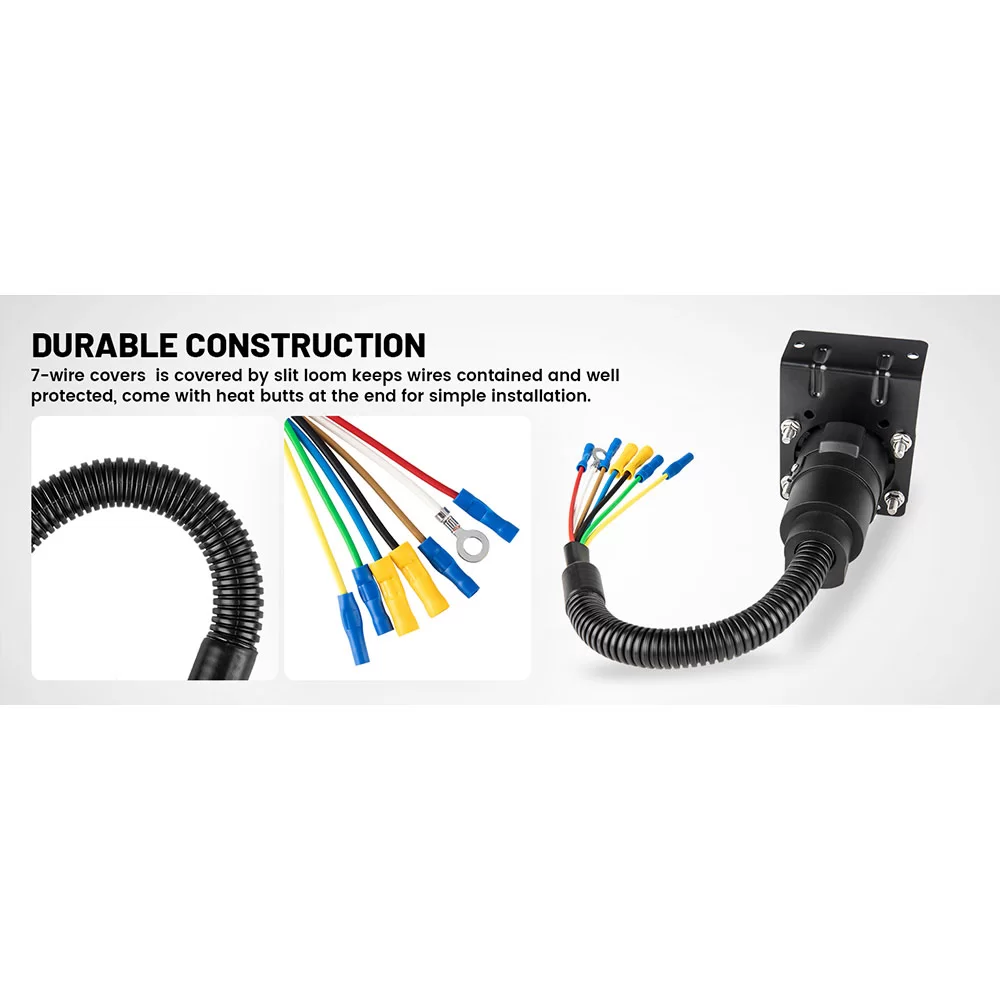
Maybe an off-the-shelf cable can't meet your needs.
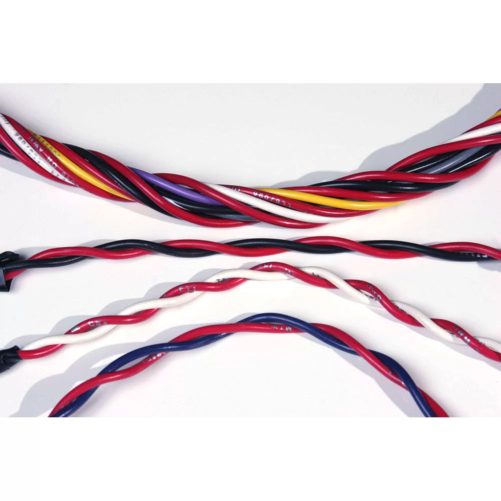
Twisting entwines multiple wires and arranges them tightly next to each other. Depending on the AWG size, we can group up to fifty conductors.
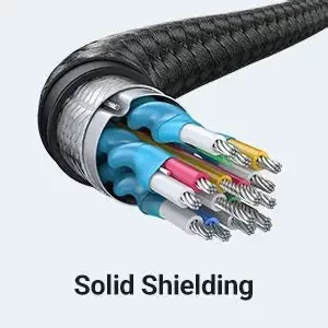
Shielding refers to the metallic layer surrounding a cable’s conductor, created to limit signal interference between the wire and external fields.
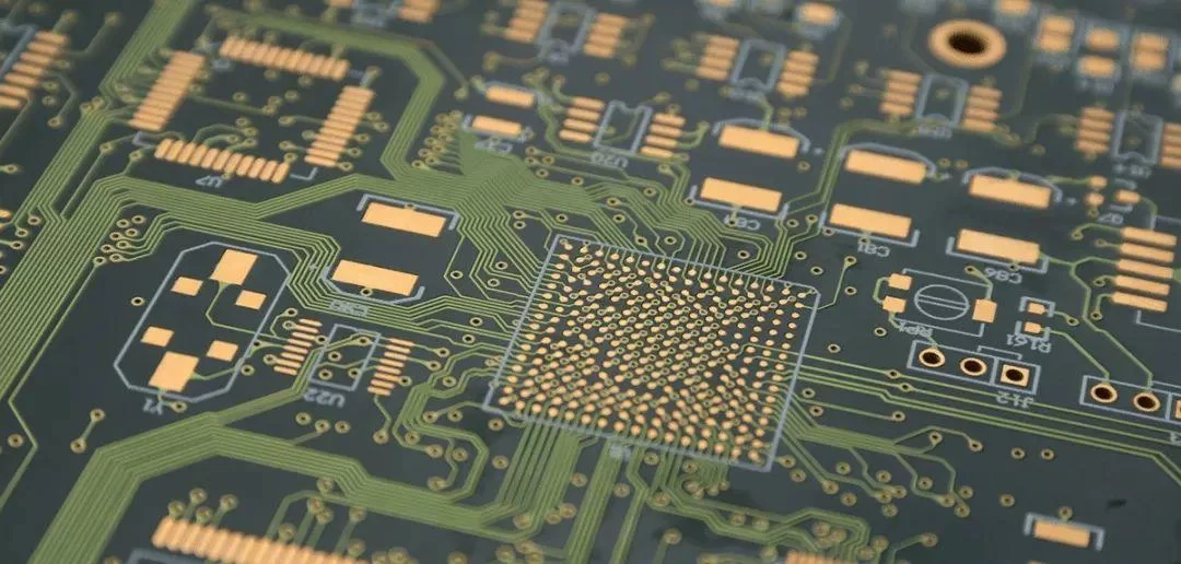
PCB manufacturing is the process of building a physical PCB from a PCB design according to a certain set of specifications.

The following design standards refer to the IPC-SM-782A standard and the design of some famous Japanese design manufacturers and some better design solutions accumulated in the manufacturing experience.
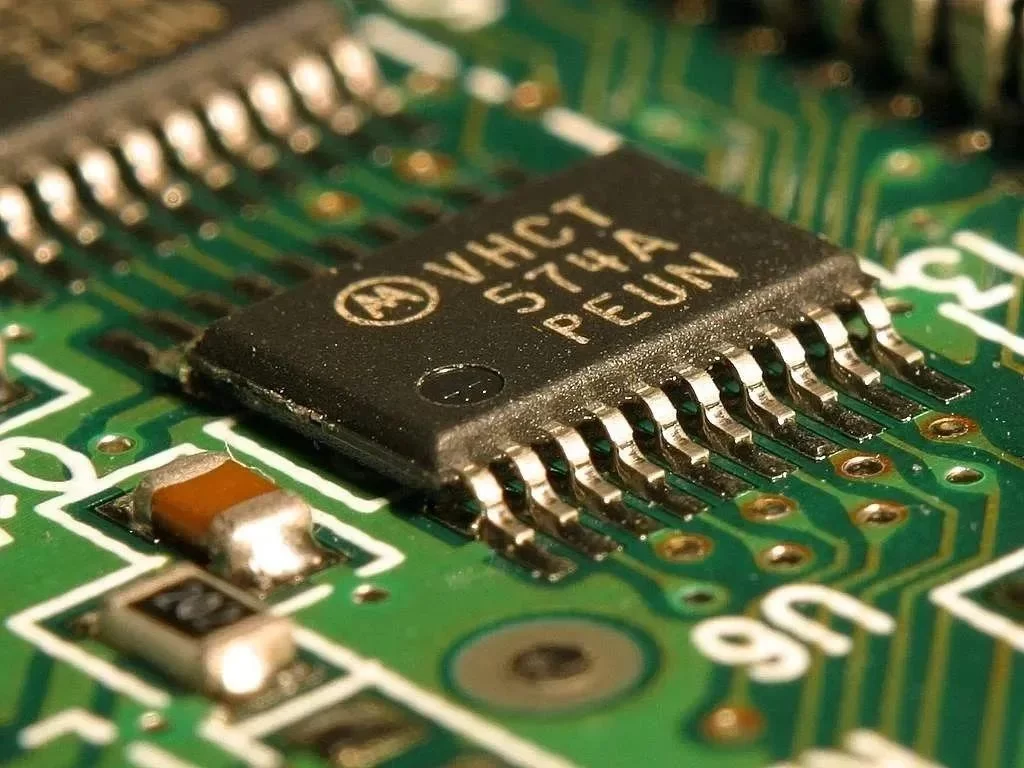
Via holes, also known as through holes, play a role in connecting different parts of a circuit board.

