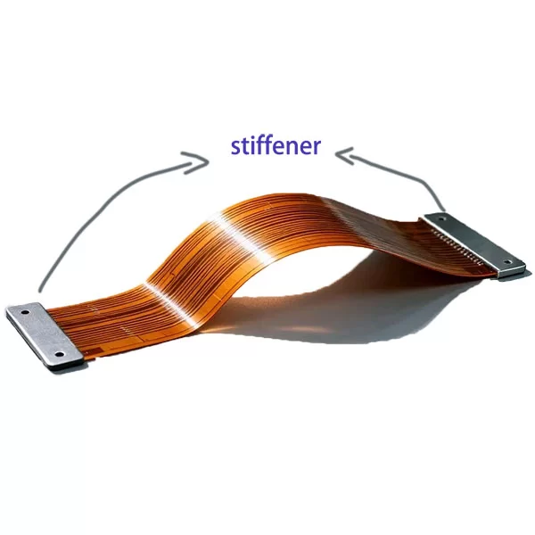
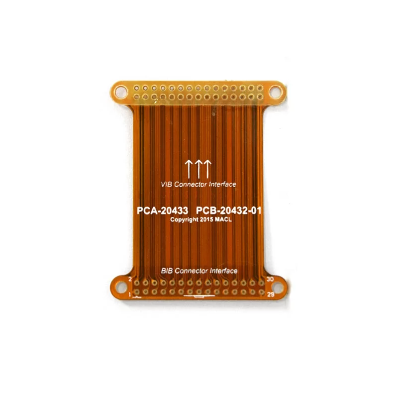
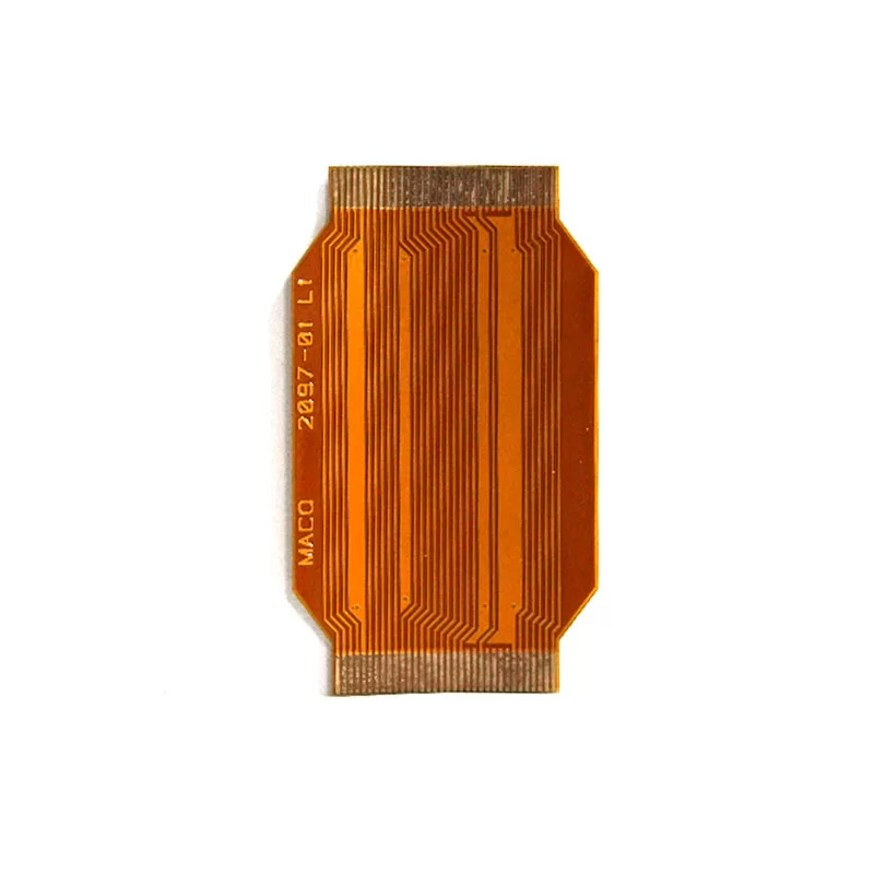
Multi-layer Flex PCBs
Data Sheet
Layer: 2L
Material: PI
Board Thickness: 0.15mm
Fr4 reinforcement: 0.2mm
Total Thickness: 0.35mm
Min Via Diameter: 0.2mm
Copper Thickness: 18μm
Trace Width/Spacing: 4/4mil
Surface Finish: ENIG1U”
What's Multilayer Flexible PCBs?
For very advanced devices that require very limited spacing or continuous movement, we need to use multi-layer flexible PCBs, This type of flexible PCB has three or more copper layers. It combines high electronic performance and cost-effectiveness and is usually used in high-tech electronic devices, such as robotics, industrial equipment, and medical applications.
Advantages of Multilayer Flexible PCBs
1. Three-Dimensional Reconfigurability
Flexible substrates (such as polyimide) enable flexible bending radii of 0.1-10mm, allowing for free folding in the X, Y, and Z axes, saving 60% space compared to rigid PCBs.
2. Breakthrough in High-Density Interconnection Performance
Utilizing microvia lamination technology, line widths/spaces can reach 20/20μm, supporting high-density stacking of 10 or more layers.
3. Adaptability to Extreme Environments
-Temperature Resistance: Operating range of -60°C to 260°C, withstanding transient high temperatures of 300°C (e.g., reflow soldering).
-Mechanical Strength: Flex life exceeding 2 million cycles (IPC-6013D standard).
-Chemical Resistance: Passes 96-hour salt spray test (ASTM B117).
4. Improved System-Level Reliability
Through integrated design, connectors are reduced by 75%, reducing the risk of solder joint failure by 90%.
5. Revolutionary Lightweighting and Thermal Management
Thickness can be compressed to 0.1mm, making it 70% lighter than rigid PCBs. The graphene composite substrate has a thermal conductivity of 600W/(m·K).
6. Smart Manufacturing Compatibility
Supports roll-to-roll automated production
Application
Multilayer FPCs are used in scenarios requiring flexible connections and high-density circuits. The core applications are as follows:
1. Consumer Electronics
Smartphones: Used for connecting displays (OLED flexible screens) to motherboards, and for wiring in camera modules and fingerprint recognition modules.
Wearable devices: Internal circuits in smartwatches and wristbands, adapting to curved wear and miniaturized designs.
Laptops: Used for connecting keyboards and touchpads to motherboards, as well as flexible circuits in screen hinges.
- 2. Automotive ElectronicsIn-Vehicle Displays: Flexible connections for central control screens, instrument clusters, and heads-up displays (HUDs), adapting to complex interior installation spaces.Sensor Connections: Circuits for cameras, radar sensors, and seat sensors, withstanding vibration and temperature fluctuations within the vehicle.New Energy Vehicles: Used for cell monitoring circuits in battery management systems (BMS), adapting to the flexible mounting requirements of battery packs.
- 3. Medical DevicesPortable Medical Devices: Internal circuits in blood glucose meters and electrocardiogram monitors, meeting the requirements for lightweight, portable devices. Implantable medical devices: such as pacemaker and neurostimulator leads, requiring flexibility, biocompatibility, and reliability.Medical imaging equipment: such as ultrasound probe internal wiring, adapting to probe bending and ensuring high-precision signal transmission.
- 4. Industrial and AerospaceIndustrial robots: Used for wiring connections at robot joints, withstanding frequent bending and mechanical movement.Aerospace equipment: such as satellites and drones, requiring lightweight circuits to accommodate space constraints and extreme environments (high and low temperatures, radiation).
Key Technical Points for Multilayer FPCs
Multilayer FPCs are more difficult to manufacture than single-layer FPCs. The core technologies are concentrated in the following three areas:
Lamination: The thickness and temperature of the interlayer insulating adhesive must be precisely controlled to ensure a tight bond between the layers and prevent air bubbles and delamination.
Plated via technology: A conductive layer is formed on the inner wall of the via through electroless copper deposition or electroplating, ensuring stable current conduction between layers. This is the core process of multilayer FPCs.
Alignment and positioning: When laminating multiple layers of substrates, strict alignment accuracy (typically within ±0.05mm) is required to prevent misalignment of circuits that could cause short circuits or open circuits.
If you have any camping barbeque equipment inquiry, please feel free to contact us.
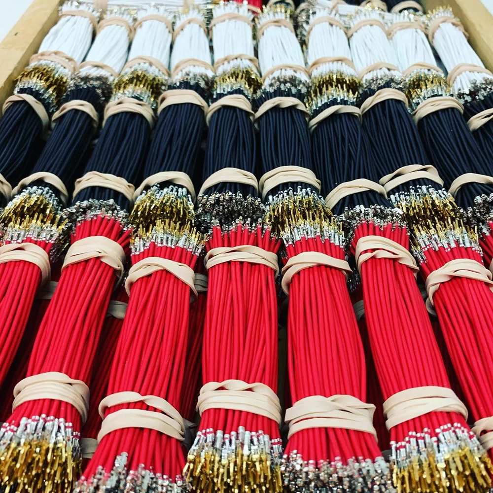
Managing kitting and packaging in-house can be time-consuming, costly, and error-prone.
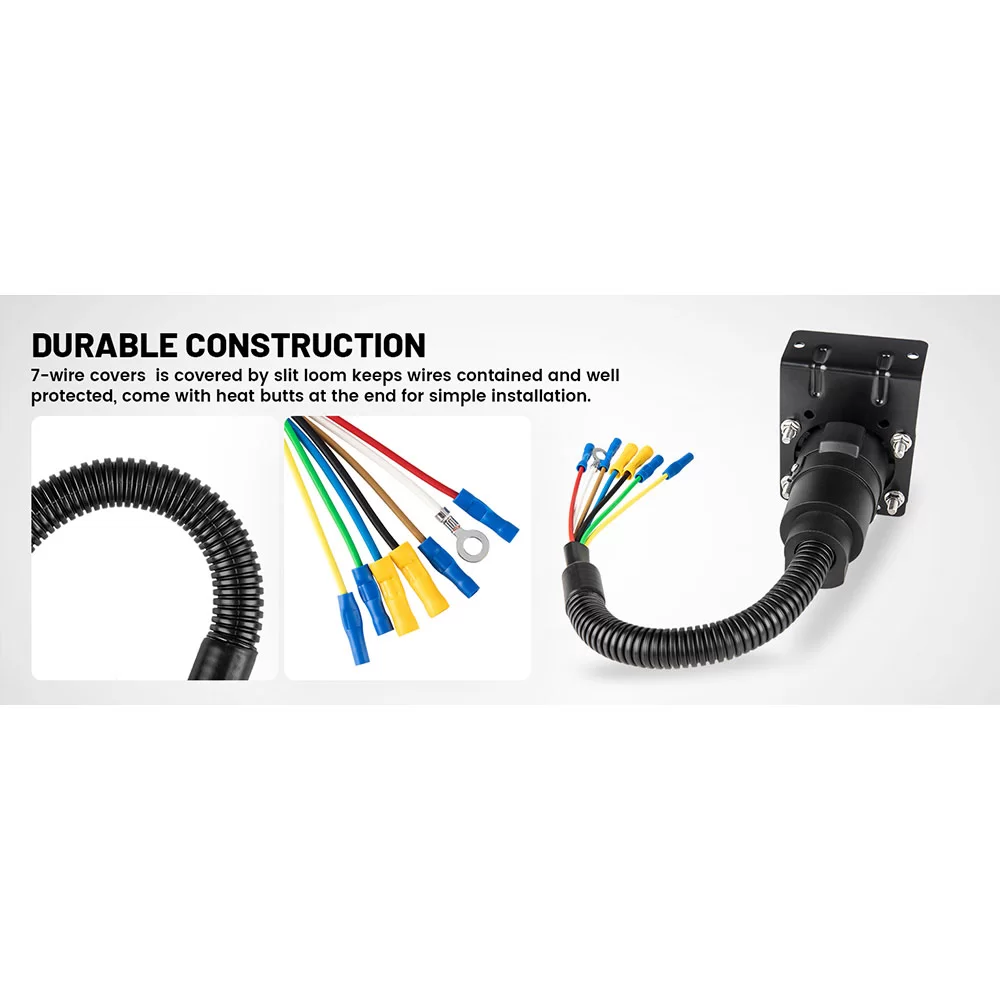
Maybe an off-the-shelf cable can't meet your needs.
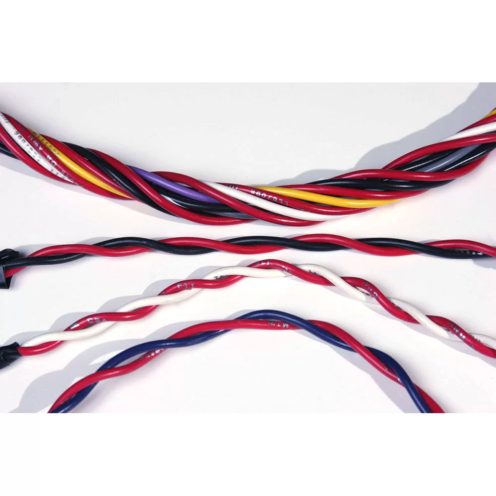
Twisting entwines multiple wires and arranges them tightly next to each other. Depending on the AWG size, we can group up to fifty conductors.
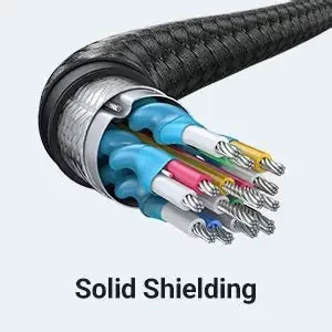
Shielding refers to the metallic layer surrounding a cable’s conductor, created to limit signal interference between the wire and external fields.
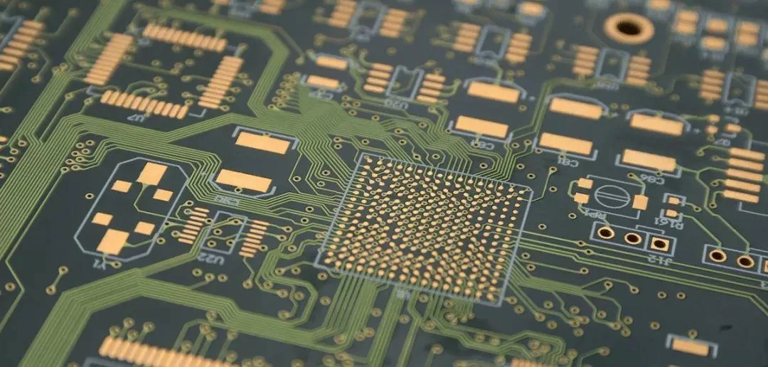
PCB manufacturing is the process of building a physical PCB from a PCB design according to a certain set of specifications.

The following design standards refer to the IPC-SM-782A standard and the design of some famous Japanese design manufacturers and some better design solutions accumulated in the manufacturing experience.
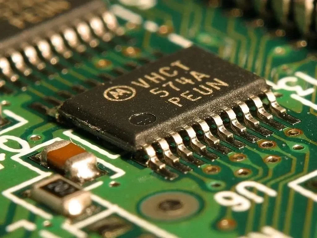
Via holes, also known as through holes, play a role in connecting different parts of a circuit board.

