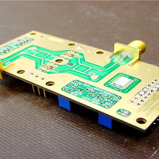
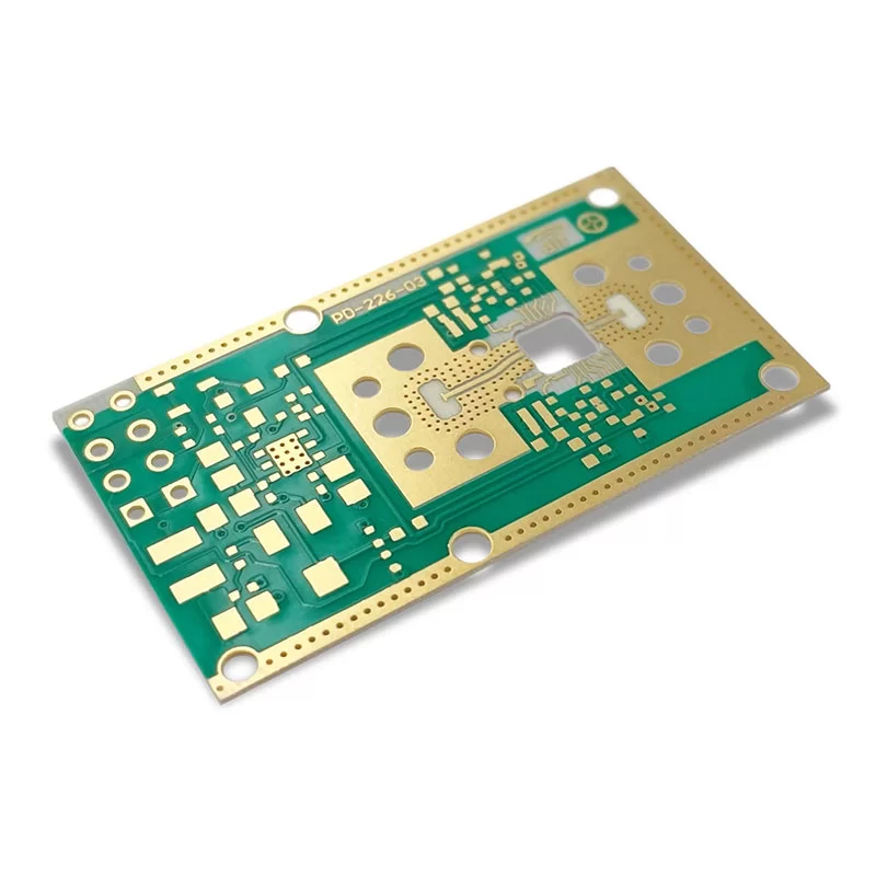
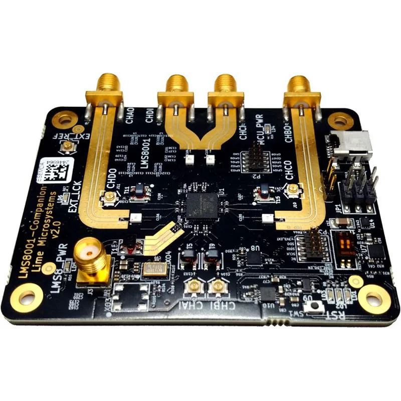
RF PCB
Data Sheet
Moduel: RF PCB
Material: FR-4,Teflon, PTFE, Ceramic, Hydrocarbon, Rogers
Quality standard: IPC Class2,Class3
PCB DK:2.0-1.6
Layers: 1-2 Layer,Multilayer PCB
Thickness:0.254mm-12mm
Copper thickness:0.5oz-2oz
Surface technology: Gold, OSP
Features: Impedance control
Application: Antenna, instrument, Equipment
Benefits
Characteristics of RF PCB
A wider range of permittivity,frompermittivity 2.0-16
- Lower loss
- More accurate impedance control
- More accurate RF circuit tolerance, minimum tolerance of Hubcircuits is ± O.02mm
- More stringent thickness control
Applications
RF Microwaves PCBs are used in various of fields,Such as Consumer Electronics / Military/Space/
/ High power /Medical / Automotive/Industrial ect.
About RF PCBs
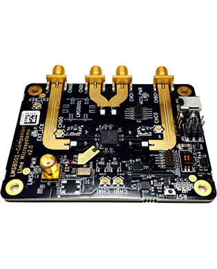
RF PCBs are circuit boards specifically designed to handle high-frequency and radio frequency signals. Compared to conventional PCBs, RF PCBs have unique design requirements to ensure efficient signal transmission at high frequencies. Impedance matching and signal integrity are crucial in RF PCB design, necessitating the use of specialized materials such as PTFE (polytetrafluoroethylene) and Rogers, which offer low dielectric loss and high thermal stability.
Basic composition of RF PCB
RF Source
RF sources are the source of RF signals. Typically, RF sources use components such as crystal oscillators to generate stable RF signals. For example, in mobile phones, RF sources generate signals of a specific frequency, providing the basis for subsequent communication. According to expert research, a stable RF source can keep frequency errors within a very small range, ensuring accurate communication.
Amplifier
Even after generating an RF signal, its strength may not be sufficient to meet actual needs. This is when an amplifier is needed. An amplifier acts like a "megaphone" for the signal, amplifying the weak RF signal to an appropriate level of intensity.
- FilterDuring RF signal transmission, various interference signals are present. Filters are used to remove these interference signals and allow only the desired signal to pass. Different types of filters can filter signals based on frequency, ensuring pure communication.
- AntennaAn antenna is a crucial component of RF circuits. It converts electrical signals into electromagnetic waves and radiates them into space, or converts electromagnetic waves in space into electrical signals. The design and performance of the antenna affect the direction, intensity, and coverage of the signal. For example, some high-gain antennas can allow signals to travel farther and cover a larger area.

If you have any camping barbeque equipment inquiry, please feel free to contact us.

Managing kitting and packaging in-house can be time-consuming, costly, and error-prone.
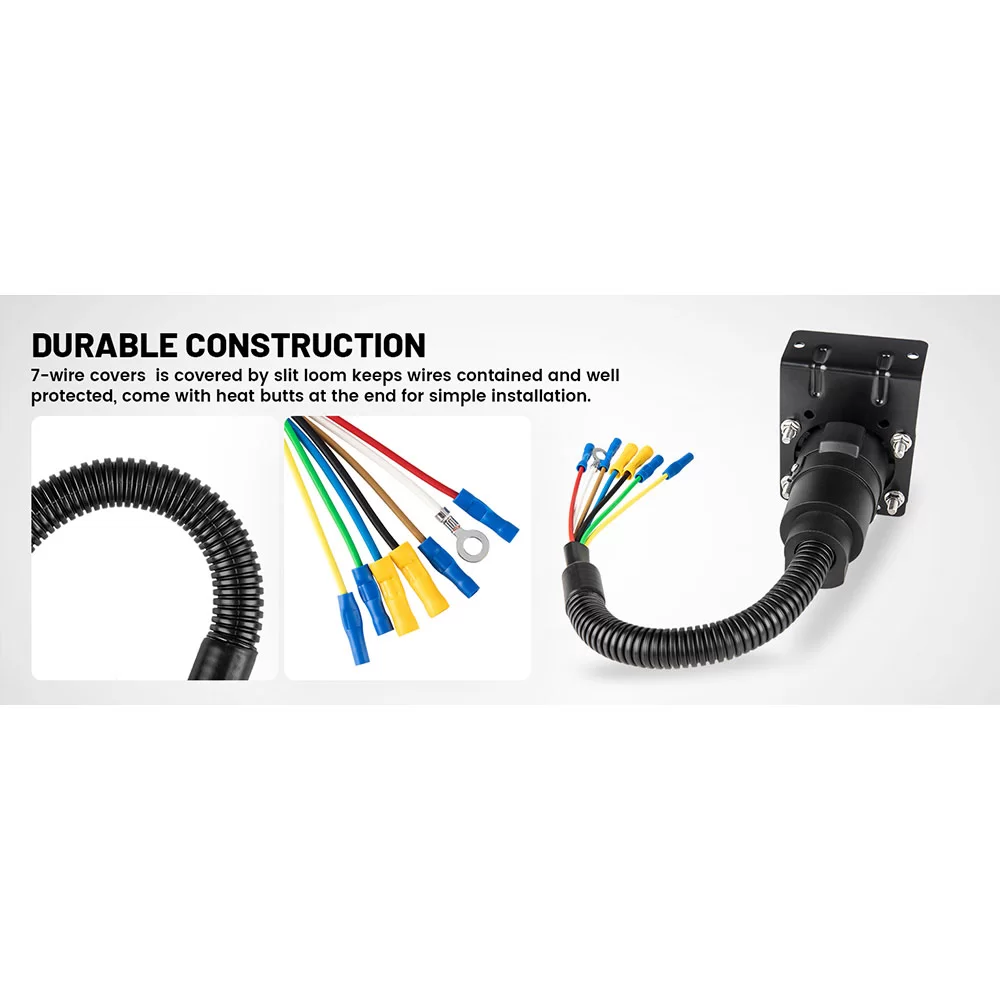
Maybe an off-the-shelf cable can't meet your needs.
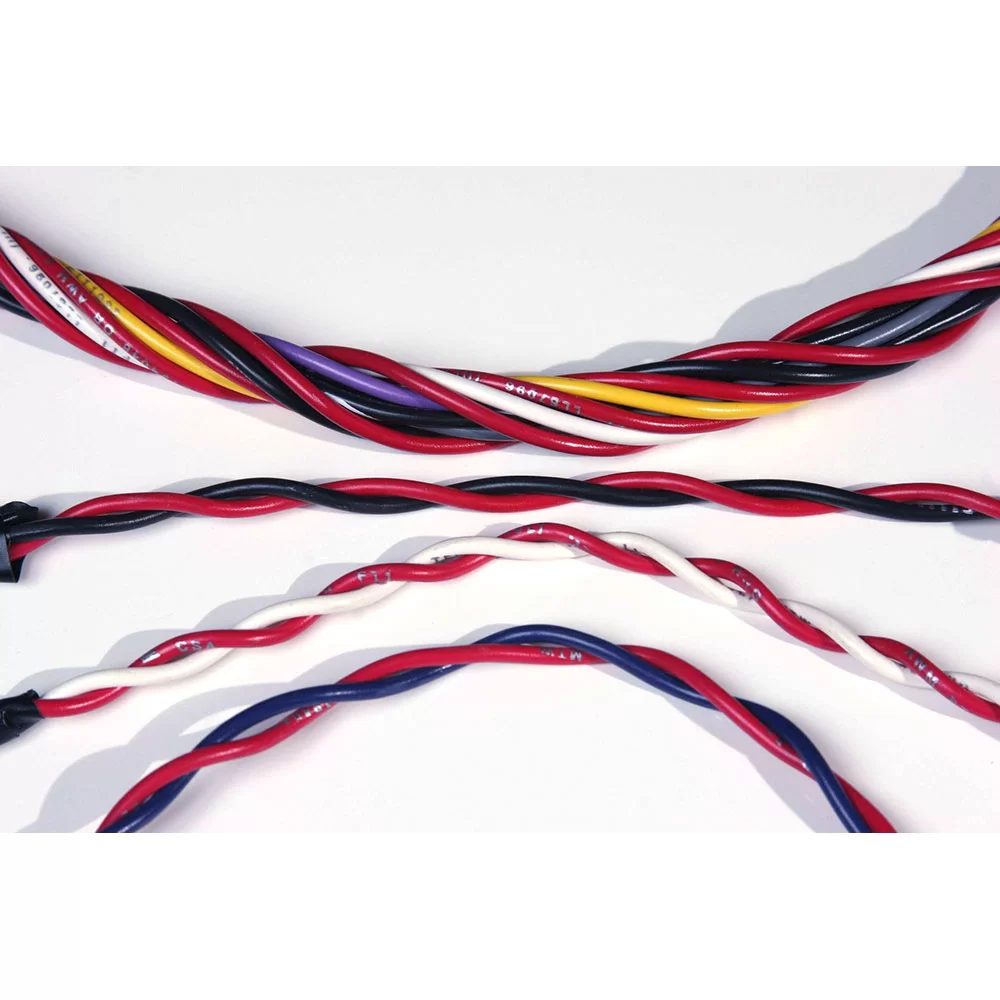
Twisting entwines multiple wires and arranges them tightly next to each other. Depending on the AWG size, we can group up to fifty conductors.

Shielding refers to the metallic layer surrounding a cable’s conductor, created to limit signal interference between the wire and external fields.
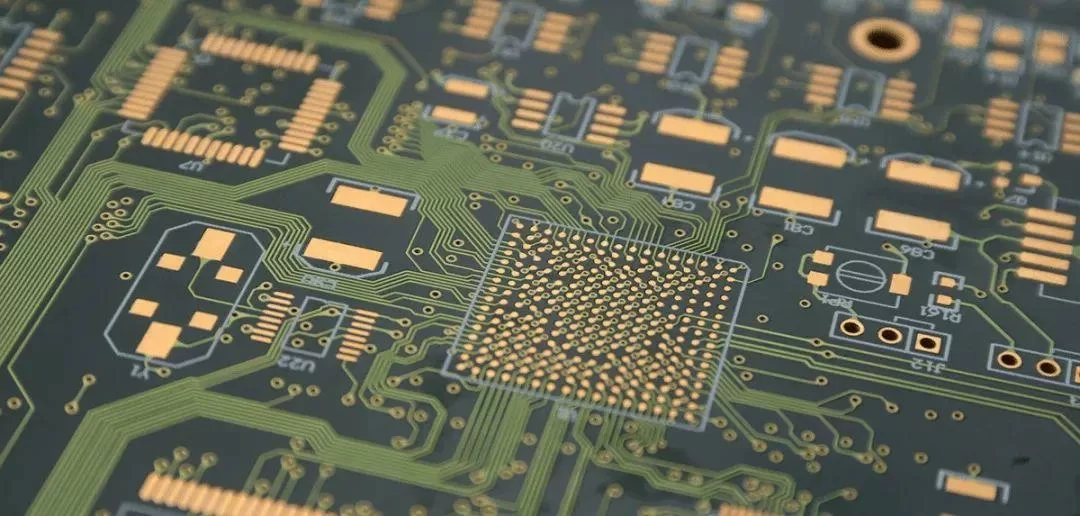
PCB manufacturing is the process of building a physical PCB from a PCB design according to a certain set of specifications.

The following design standards refer to the IPC-SM-782A standard and the design of some famous Japanese design manufacturers and some better design solutions accumulated in the manufacturing experience.
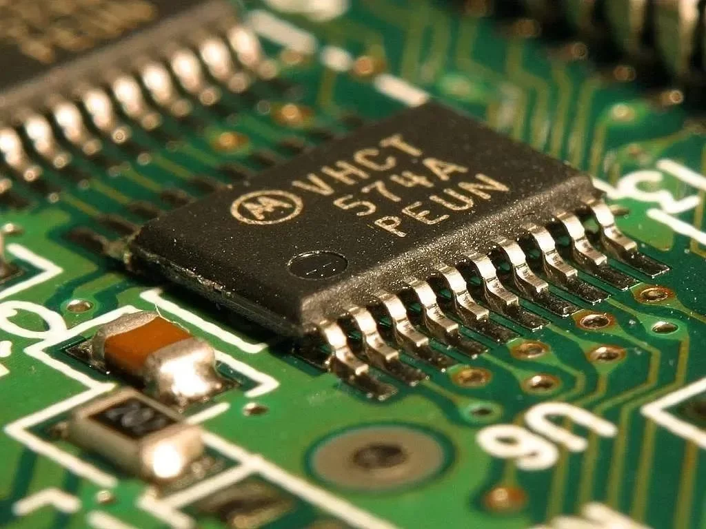
Via holes, also known as through holes, play a role in connecting different parts of a circuit board.

