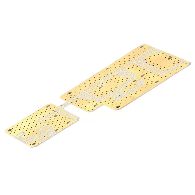
Silicon Carbide PCB
About Silicon Carbide PCB
Silicon carbide ceramic circuit boards have attracted considerable attention for their superior thermal conductivity, high-temperature and high-voltage resistance, wear resistance, low loss, and high operating frequency.
Silicon carbide's high bandgap width contributes to its high breakdown field and high operating temperature. Therefore, silicon carbide ceramic circuit boards are suitable for products requiring high heat dissipation, high thermal conductivity, high current, high voltage, and high-frequency operation.
However, the current manufacturing cost of silicon carbide remains high, but with advancements in manufacturing technology, its application prospects are promising.
Development in Ceramic PCBs
High-thermal-conductivity ceramic materials: For example, modified AlN materials can further increase thermal conductivity to 200–250 W/m·K; Multilayer ceramic substrates: Enable high-density circuit routing and three-dimensional integration, increasing functional integration;
Smart manufacturing and process monitoring: Digitally monitor lamination, brazing, and thick film parameters to achieve highly consistent production; Environmentally friendly and safe materials: Reduce the use of toxic materials, such as alternatives to beryllium oxide;
Customized applications: Provide customized solutions for high-performance ceramic-based PCBs based on power density and thermal management requirements.
Advantages Silicon Nitride
-High strength over a wide temperature range
-High fracture toughness / flexural strength
-Outstanding wear resistance, both impingement as well as frictional modes
-Good thermal shock resistance (low expansion rate + high thermal conductivity)
-Strong chemical resistance
-high absorption
Description
Silicon Nitride substrates have the best mix of electrical, thermal, and mechanical properties of any ceramic material. It is the choice of material for applications where other ceramics prove to be too weak to handle mechanical stress or thermal shocks but you still need to handle high current, conduct heat, or withstand chemical hazards. Examples are battery management systems for electrical drivetrains, high-pressure environments like deep-sea sensors, industrial sensors & antennae, portable lighting & scanning solutions.
If you have any camping barbeque equipment inquiry, please feel free to contact us.
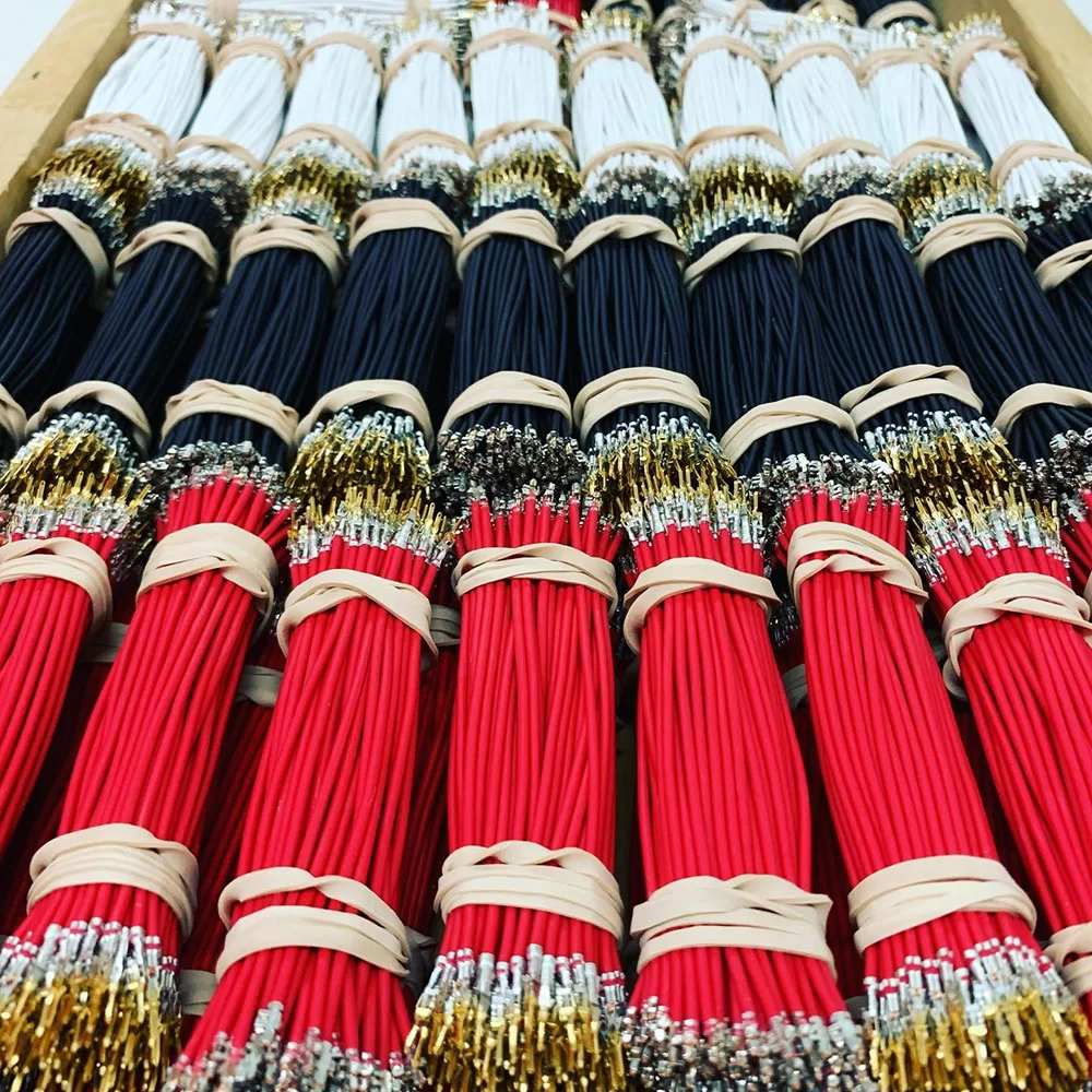
Managing kitting and packaging in-house can be time-consuming, costly, and error-prone.
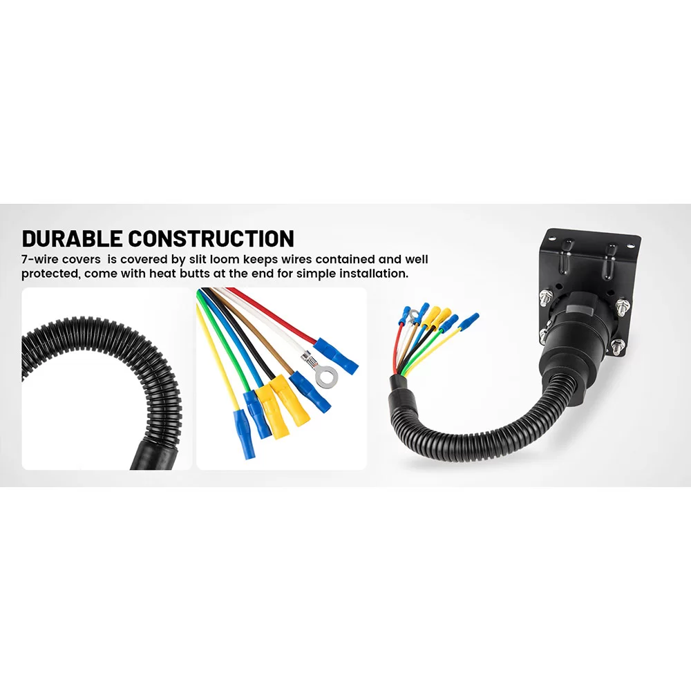
Maybe an off-the-shelf cable can't meet your needs.
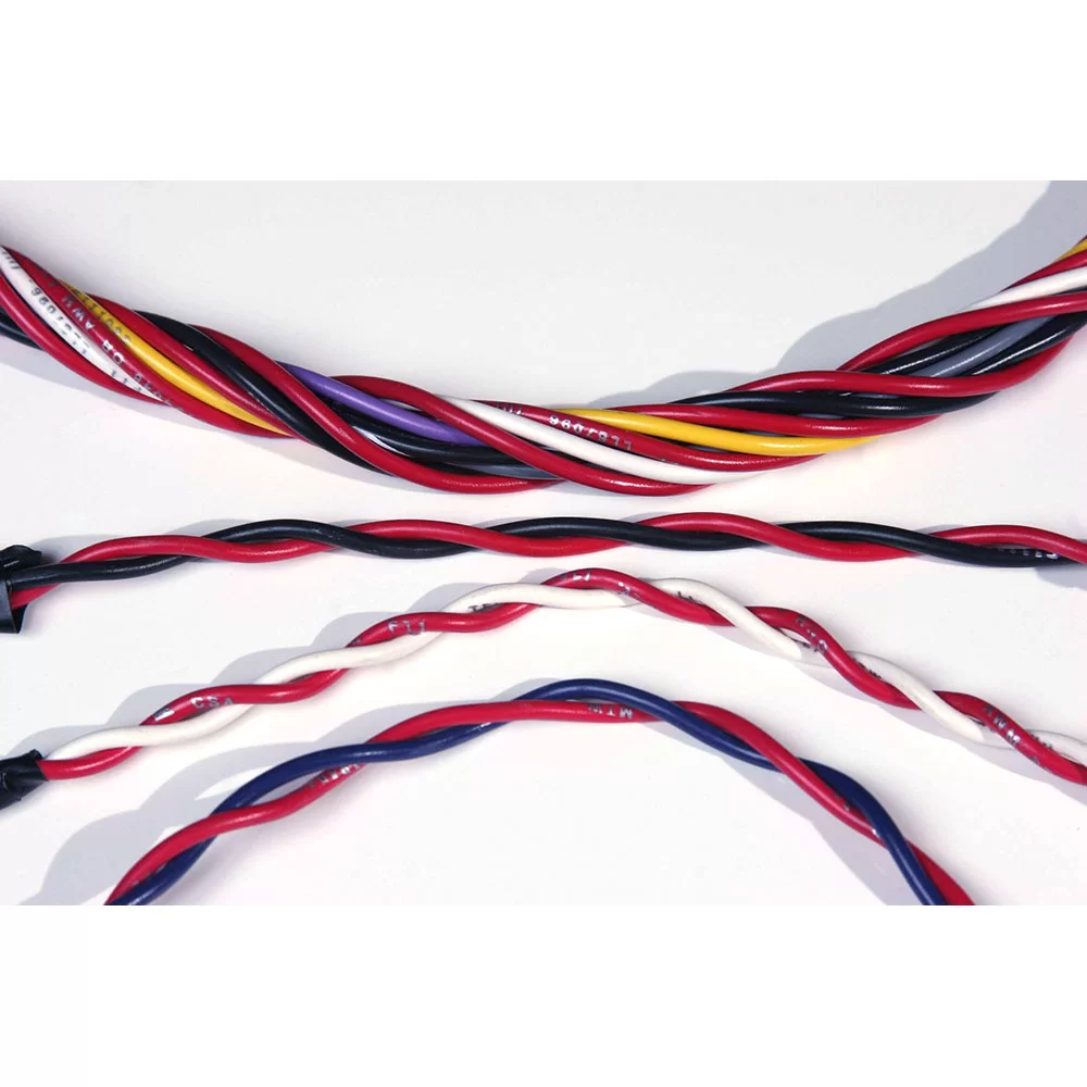
Twisting entwines multiple wires and arranges them tightly next to each other. Depending on the AWG size, we can group up to fifty conductors.
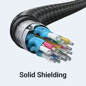
Shielding refers to the metallic layer surrounding a cable’s conductor, created to limit signal interference between the wire and external fields.
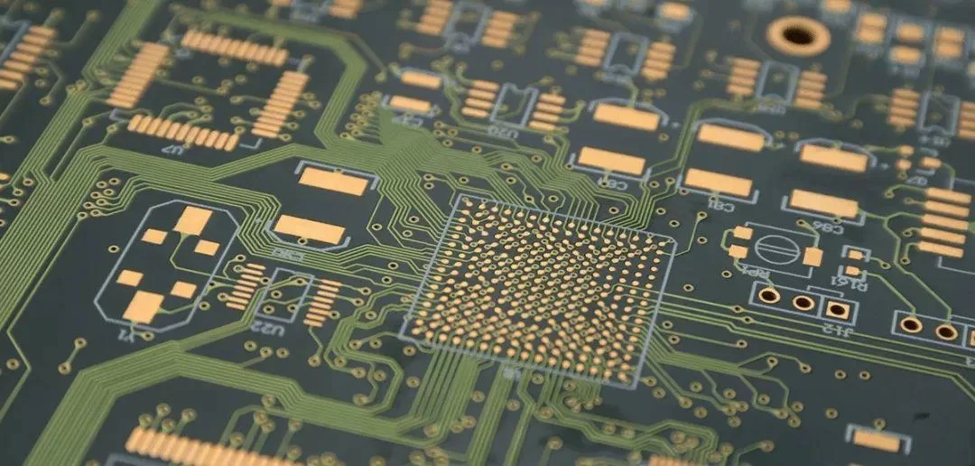
PCB manufacturing is the process of building a physical PCB from a PCB design according to a certain set of specifications.

The following design standards refer to the IPC-SM-782A standard and the design of some famous Japanese design manufacturers and some better design solutions accumulated in the manufacturing experience.
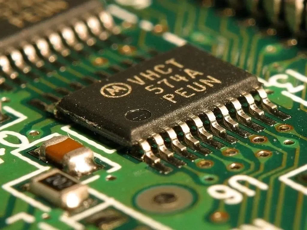
Via holes, also known as through holes, play a role in connecting different parts of a circuit board.

